|
|
|
PDF HI-574 Data sheet ( Hoja de datos )
| Número de pieza | HI-574 | |
| Descripción | Complete/ 12-Bit A/D Converters with Microprocessor Interface | |
| Fabricantes | Intersil Corporation | |
| Logotipo | ||
Hay una vista previa y un enlace de descarga de HI-574 (archivo pdf) en la parte inferior de esta página. Total 18 Páginas | ||
|
No Preview Available !
August 1997
HI-574A, HI-674A,
HI-774
Complete, 12-Bit A/D Converters
with Microprocessor Interface
Features
• Complete 12-Bit A/D Converter with Reference and Clock
• Full 8-Bit, 12-Bit or 16-Bit Microprocessor Bus Interface
• Bus Access Time . . . . . . . . . . . . . . . . . . . . . . . . . . 150ns
• No Missing Codes Over Temperature
• Minimal Setup Time for Control Signals
• Fast Conversion Times
- HI-574A (Max) . . . . . . . . . . . . . . . . . . . . . . . . . . . . 25µs
- HI-674A (Max) . . . . . . . . . . . . . . . . . . . . . . . . . . . . 15µs
- HI-774 (Max) . . . . . . . . . . . . . . . . . . . . . . . . . . . . . . 9µs
• Digital Error Correction (HI-774)
• Low Noise, via Current-Mode Signal
Transmission Between Chips
• Byte Enable/Short Cycle (AO Input)
- Guaranteed Break-Before-Make Action, Eliminating
Bus Contention During Read Operation. Latched by
Start Convert Input (To Set the Conversion Length)
• Supply Voltage . . . . . . . . . . . . . . . . . . . . . ±12V to ±15V
Applications
• Military and Industrial Data Acquisition Systems
• Electronic Test and Scientific Instrumentation
• Process Control Systems
Description
The HI-X74(A) is a complete 12-bit, Analog-to-Digital
Converter, including a +10V reference clock, three-state out-
puts and a digital interface for microprocessor control. Succes-
sive approximation conversion is performed by two monolithic
dice housed in a 28 lead package. The bipolar analog die fea-
tures the Intersil Dielectric Isolation process, which provides
enhanced AC performance and freedom from latch-up.
Custom design of each IC (bipolar analog and CMOS digital)
has yielded improved performance over existing versions of
this converter. The voltage comparator features high PSRR
plus a high speed current-mode latch, and provides precise
decisions down to 0.1 LSB of input overdrive. More than 2X
reduction in noise has been achieved by using current
instead of voltage for transmission of all signals between the
analog and digital ICs. Also, the clock oscillator is current
controlled for excellent stability over temperature.
The HI-X74(A) offers standard unipolar and bipolar input
ranges, laser trimmed for specified linearity, gain and offset
accuracy. The low noise buried zener reference circuit is
trimmed for minimum temperature coefficient.
Power requirements are +5V and ±12V to ±15V, with typical
dissipation of 385mW (HI-574A/674A) and 390mW (HI-774) at
12V. All models are available in sidebrazed DIP, PDIP, and
CLCC. For additional HI-Rel screening including 160 hour burn-
in, specify “-8” suffix. For MIL-STD-883 compliant parts, request
HI-574A/883, HI-674A/883, and HI-774/883 data sheets.
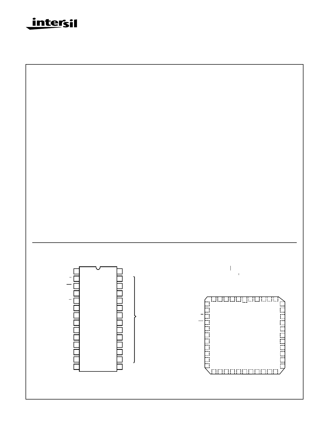
Pinouts
(PDIP, SBDIP)
TOP VIEW
(CLCC)
TOP VIEW
+5V SUPPLY, VLOGIC 1
DATA MODE SEL, 12/8 2
CHIP SEL, CS
BYTE ADDR/SHORT
CYCLE, AO
READ/CONVERT, R/C
3
4
5
CHIP ENABLE, CE 6
+12V/+15V SUPPLY, VCC 7
+10V REF, REF OUT 8
ANALOG
COMMON, AC
9
REFERENCE INPUT 10
-12V/-15V SUPPLY, VEE 11
BIPOLAR OFFSET
BIP OFF
12
10V INPUT 13
20V INPUT 14
28 STATUS, STS
27 DB11 MSB
26 DB10
25 DB9
24 DB8
23 DB7
22 DB6
21 DB5
DIGITAL
DATA
OUTPUTS
20 DB4
19 DB3
18 DB2
17 DB1
16 DB0 LSB
15
DIG COMMON,
DC
6 5 4 3 2 1 44 43 42 41 40
NC 7
39 NC
NC 8
38 NC
READ CONVERT, R/C 9
37 DB9
CHIP ENABLE, CE 10
36 DB8
+15V SUPPLY, VCC 11
+10V REFERENCE,
REF OUT
12
ANALOG COMMON, AC 13
REFERENCE INPUT,
REF IN
14
-15V SUPPLY, VEE 15
NC 16
BIPOLAR OFFSET, 17
BIP OFF
18 19 20 21 22 23 24 25 26 27 28
35 DB7
34 DB6
33 DB5
32 DB4
31 DB3
30 NC
29 DB2
CAUTION: These devices are sensitive to electrostatic discharge; follow proper IC Handling Procedures.
1-888-INTERSIL or 321-724-7143 | Copyright © Intersil Corporation 1999
6-952
File Number 3096.4
1 page 
HI-574A, HI-674A, HI-774
DC and Transfer Accuracy Specifications Typical at 25oC with VCC = +15V or +12V, VLOGIC = +5V, VEE = -15V or -12V,
Unless Otherwise Specified (Continued)
PARAMETER
Temperature Coefficients
Guaranteed Max Change, TMIN to TMAX (Using Internal Reference)
Unipolar Offset
HI-574A, HI-674A
HI-774
Bipolar Offset
HI-574A, HI-674A
HI-774
Full Scale Calibration HI-574A, HI-674A
HI-774
Power Supply Rejection
Max Change In Full Scale Calibration
+13.5V < VCC < +16.5V or +11.4V < VCC < +12.6V
+4.5V < VLOGIC < +5.5V
-16.5V < VEE < -13.5V or -12.6V < VEE < -11.4V
ANALOG INPUTS
Input Ranges
Bipolar
Unipolar
Input Impedance
10V Span
20V Span
POWER SUPPLIES
Operating Voltage Range
VLOGIC
VCC
VEE
Operating Current
ILOGIC
ICC +15V Supply
IEE -15V Supply
Power Dissipation
±15V, +15V
±12V, +5V
Internal Reference Voltage
TMIN to TMAX
Output Current, Available For External Loads (External Load Should
Not Change During Conversion).
TEMPERATURE RANGE
-5 (0oC to 75oC)
J SUFFIX K SUFFIX L SUFFIX
±2 ±1 ±1
±2 ±1 ±1
±2 ±1 ±1
±2 ±2 ±1
±9 ±2 ±2
±9 ±5 ±2
±2 ±1 ±1
±1/2 ±1/2 ±1/2
±2 ±1 ±1
-5 to +5
-10 to +10
0 to +10
0 to +20
5K, ±25%
10K, ±25%
+4.5 to +5.5
+11.4 to +16.5
-11.4 to -16.5
7 Typ, 15 Max
11 Typ, 15 Max
21 Typ, 28 Max
515 Typ, 720 Max
385 Typ
+10.00 ±0.05 Max
2.0 Max
UNITS
LSB
LSB
LSB
LSB
LSB
LSB
LSB
LSB
LSB
V
V
V
V
Ω
Ω
V
V
V
mA
mA
mA
mW
mW
V
mA
6-956
5 Page 
HI-574A, HI-674A, HI-774
Temperature Coefficients
The temperature coefficients for full-scale calibration, unipo-
lar offset, and bipolar offset specify the maximum change
from the initial (25oC) value to the value at TMIN or TMAX.
Power Supply Rejection
The standard specifications for the HI-X74A assume use of
+5.00V and ±15.00V or ±12.00V supplies. The only effect of
power supply error on the performance of the device will be
a small change in the full scale calibration. This will result in
a linear change in all lower order codes. The specifications
show the maximum change in calibration from the initial
value with the supplies at the various limits.
Code Width
A fundamental quantity for A/D converter specifications is
the code width. This is defined as the range of analog input
values for which a given digital output code will occur. The
nominal value of a code width is equivalent to 1 least signifi-
cant bit (LSB) of the full scale range or 2.44mV out of 10V for
a 12-bit ADC.
Quantization Uncertainty
Analog-to-digital converters exhibit an inherent quantization
uncertainty of ±1/2 LSB. This uncertainty is a fundamental
characteristic of the quantization process and cannot be
reduced for a converter of given resolution.
Left-justified Data
The data format used in the HI-X74(A) is left-justified. This
means that the data represents the analog input as a frac-
tion of full-scale, ranging from 0 to 4095 . This implies a
binary point to the left of the MSB. 4096
Applying the HI-X74(A)
For each application of this converter, the ground
connections, power supply bypassing, analog signal source,
digital timing and signal routing on the circuit board must be
optimized to assure maximum performance. These areas
are reviewed in the following sections, along with basic oper-
ating modes and calibration requirements.
Physical Mounting and Layout Considerations
Layout
Unwanted, parasitic circuit components, (L, R, and C) can
make 12-bit accuracy impossible, even with a perfect A/D
converter. The best policy is to eliminate or minimize these
parasitics through proper circuit layout, rather than try to
quantify their effects.
The recommended construction is a double-sided printed
circuit board with a ground plane on the component side.
Other techniques, such as wire-wrapping or point-to-point
wiring on vector board, will have an unpredictable effect on
accuracy.
In general, sensitive analog signals should be routed between
ground traces and kept well away from digital lines. If analog
and digital lines must cross, they should do so at right angles.
Power Supplies
Supply voltages to the HI-X74(A) (+15V, -15V and +5V) must
be “quiet” and well regulated. Voltage spikes on these lines can
affect the converter’s accuracy, causing several LSBs to flicker
when a constant input is applied. Digital noise and spikes from
a switching power supply are especially troublesome. If switch-
ing supplies must be used, outputs should be carefully filtered
to assure “quiet” DC voltage at the converter terminals.
Further, a bypass capacitor pair on each supply voltage
terminal is necessary to counter the effect of variations in
supply current. Connect one pair from pin 1 to 15 (VLOGIC
supply), one from pin 7 to 9 (VCC to Analog Common) and
one from pin 11 to 9 (VEE to Analog Common). For each
capacitor pair, a 10µF tantalum type in parallel with a 0.1µF
ceramic type is recommended.
Ground Connections
Pins 9 and 15 should be tied together at the package to
guarantee specified performance for the converter. In
addition, a wide PC trace should run directly from pin 9 to
(usually) +15V common, and from pin 15 to (usually) the +5V
Logic Common. If the converter is located some distance from
the system’s “single point” ground, make only these connec-
tions to pins 9 and 15: Tie them together at the package, and
back to the system ground with a single path. This path
should have low resistance. (Code dependent currents flow in
the VCC, VEE and VLOGIC terminals, but not through the
HI-X74(A)’s Analog Common or Digital Common).
Analog Signal Source
HI-574A and HI-674A
The device chosen to drive the HI-X74A analog input will see a
nominal load of 5kΩ (10V range) or 10kΩ (20V range).
However, the other end of these input resistors may change
±400mV with each bit decision, creating abrupt changes in cur-
rent at the analog input. Thus, the signal source must maintain
its output voltage while furnishing these step changes in load
current, which occur at 1.6µs and 950ns intervals for the
HI-574A and HI-674A, respectively. This requires low output
impedance and fast settling by the signal source.
The output impedance of an op amp, for example, has an open
loop value which, in a closed loop, is divided by the loop gain
available at a frequency of interest. The amplifier should have
acceptable loop gain at 600KHz for use with the HI-X74A. To
check whether the output properties of a signal source are
suitable, monitor the HI-X74A’s input (pin 13 or 14) with an oscil-
loscope while a conversion is in progress. Each of the twelve
disturbances should subside in 1µs or less for the HI-574A and
500ns or less for the HI-674A. (The comparator decision is
made about 1.5µs and 850ns after each code change from the
SAR for the HI-574A and HI-674A, respectively.)
If the application calls for a Sample/Hold to precede the
converter, it should be noted that not all Sample/Holds are
compatible with the HI-574A in the manner described above.
These will require an additional wideband buffer amplifier to
lower their output impedance. A simpler solution is to use the
Intersil HA-5320 Sample/Hold, which was designed for use
with the HI-574A.
6-962
11 Page | ||
| Páginas | Total 18 Páginas | |
| PDF Descargar | [ Datasheet HI-574.PDF ] | |
Hoja de datos destacado
| Número de pieza | Descripción | Fabricantes |
| HI-5701 | 6-Bit/ 30MSPS/ Flash A/D Converter | Intersil Corporation |
| HI-574 | Complete/ 12-Bit A/D Converters with Microprocessor Interface | Intersil Corporation |
| HI-574A | Complete/ 12-Bit A/D Converters with Microprocessor Interface | Intersil Corporation |
| Número de pieza | Descripción | Fabricantes |
| SLA6805M | High Voltage 3 phase Motor Driver IC. |
Sanken |
| SDC1742 | 12- and 14-Bit Hybrid Synchro / Resolver-to-Digital Converters. |
Analog Devices |
|
DataSheet.es es una pagina web que funciona como un repositorio de manuales o hoja de datos de muchos de los productos más populares, |
| DataSheet.es | 2020 | Privacy Policy | Contacto | Buscar |