|
|
|
PDF TNY288K Data sheet ( Hoja de datos )
| Número de pieza | TNY288K | |
| Descripción | (TNY284 - TNY290) Off-Line Switcher | |
| Fabricantes | Power Integrations | |
| Logotipo | ||
Hay una vista previa y un enlace de descarga de TNY288K (archivo pdf) en la parte inferior de esta página. Total 26 Páginas | ||
|
No Preview Available !
TNY284-290
TinySwitch™-4 Family
Energy-Efficient, Off-Line Switcher with
Line Compensated Overload Power
Product Highlights
Lowest System Cost with Enhanced Flexibility
• 725 V rated MOSFET
• Increases BV de-rating margin
• Line compensated overload power – no additional components
• Dramatically reduces max overload variation over universal input
voltage range
• ±5% turn on UV threshold: line voltage sense with single external
resistor
• Simple ON/OFF control, no loop compensation needed
• Selectable current limit through BP/M capacitor value
• Higher current limit extends peak power or, in open frame
applications, maximum continuous power
• Lower current limit improves efficiency in enclosed adapters/
chargers
• Allows optimum TinySwitch-4 choice by swapping devices with no
other circuit redesign
• Tight I2f parameter tolerance reduces system cost
• Maximizes MOSFET and magnetics utilization
• ON-time extension – extends low-line regulation range/hold-up time
to reduce input bulk capacitance
• Self-biased: no bias winding or bias components
• Frequency jittering reduces EMI filter costs
• Pin-out simplifies heat sinking to the PCB
• SOURCE pins are electrically quiet for low EMI
Enhanced Safety and Reliability Features
• Accurate hysteretic thermal shutdown protection with automatic
recovery eliminates need for manual reset
• Auto-restart delivers <3% of maximum power in short-circuit and
open loop fault conditions
• Output overvoltage shutdown with optional Zener
• Fast AC reset with optional UV external resistor
• Very low component count enhances reliability and enables
single-sided printed circuit board layout
• High bandwidth provides fast turn-on with no overshoot and
excellent transient load response
• Extended creepage between DRAIN and all other pins improves field
reliability
EcoSmart™– Extremely Energy Efficient
• Easily meets all global energy efficiency regulations
• No-load <30 mW with bias winding, <150 mW at 265 VAC without
bias winding
• ON/OFF control provides constant efficiency down to very light loads
– ideal for mandatory CEC regulations and EuP standby requirements
Applications
• PC Standby and other auxiliary supplies
• DVD/PVR and other low power set top decoders
• Supplies for appliances, industrial systems, metering, etc
• Chargers/adapters for cell/cordless phones, PDAs, digital cameras,
MP3/portable audio, shavers, etc.
+
Wide-Range
High-Voltage
DC Input
D
TinySwitch-4
S
EN/UV
BP/M
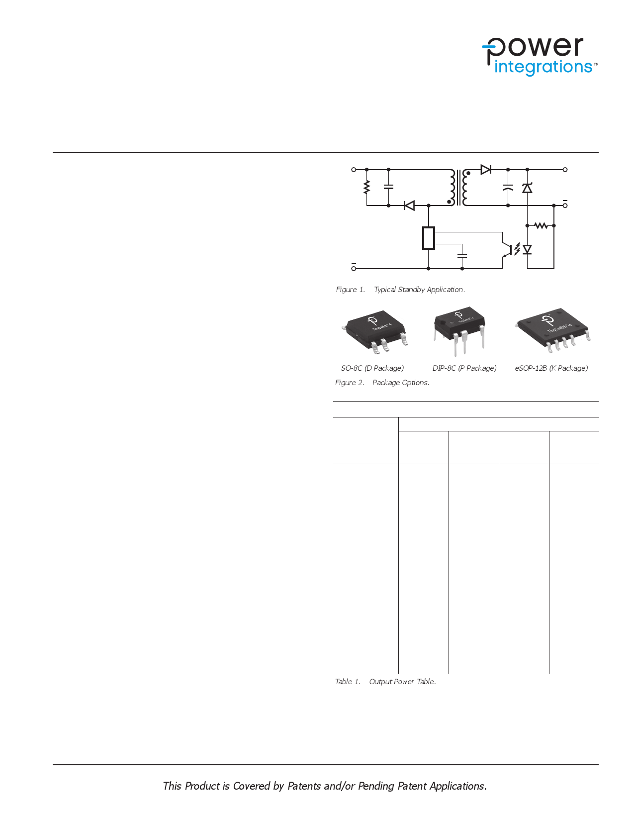
Figure 1. Typical Standby Application.
+
DC
Output
PI-6578-020915
SO-8C (D Package)
DIP-8C (P Package)
Figure 2. Package Options.
eSOP-12B (K Package)
Output Power Table
Product3
230 VAC ± 15%
Adapter1
Peak or
Open
Frame2
85-265 VAC
Adapter1
Peak or
Open
Frame2
TNY284P/D/K
TNY285P/D
TNY285K
6W
8.5 W
11 W
11 W
15 W
15 W
5W
6W
7.5 W
8.5 W
11.5 W
11.5 W
TNY286P/D
10 W
19 W
7W
15 W
TNY286K
13.5 W
19 W
9.5 W
15 W
TNY287P
13 W
23.5 W
8W
18 W
TNY287D
11.5 W
23.5 W
7W
18 W
TNY287K
TNY288P
TNY288D
TNY288K
TNY289P
18 W
16 W
14.5 W
23 W
18 W
23.5 W
28 W
26 W
28 W
32 W
11 W
10 W
9W
14.5 W
12 W
18 W
21.5 W
19.5 W
21.5 W
25 W
TNY289K
25 W
32 W
17 W
25 W
TNY290P
20 W
36.5 W
14 W
28.5 W
TNY290K
28 W
36.5 W
20 W
28.5 W
Table 1. Output Power Table.
Notes:
1. Minimum continuous power in a typical non-ventilated enclosed adapter
measured at +50 °C ambient. Use of an external heat sink will increase power
capability.
2. Minimum peak power capability in any design or minimum continuous power
in an open frame design (see Key Applications Considerations).
3. Packages: P: DIP-8C, D: SO-8C, K: eSOP-12B. See Part Ordering Information.
www.power.com
This Product is Covered by Patents and/or Pending Patent Applications.
February 2015
1 page 
TNY284-290
percentage of cycles will occur to satisfy the power consumption of
the power supply.
The response time of the ON/OFF control scheme is very fast
compared to PWM control. This provides tight regulation and
excellent transient response.
Power-Up/Down
The TinySwitch-4 requires only a 0.1 μF capacitor on the BYPASS/
MULTI-FUNCTION pin to operate with standard current limit.
Because of its small size, the time to charge this capacitor is kept to
an absolute minimum, typically 0.6 ms. The time to charge will vary
in proportion to the BYPASS/MULTI-FUNCTION pin capacitor value
when selecting different current limits. Due to the high bandwidth
of the ON/OFF feedback, there is no overshoot at the power supply
output. When an external resistor (4 MW) is connected from the
positive DC input to the ENABLE/UNDERVOLTAGE pin, the power
MOSFET switching will be delayed during power-up until the DC line
voltage exceeds the threshold (100 V). Figures 11 and 12 show the
power-up timing waveform in applications with and without an
external resistor (4 MW) connected to the ENABLE/UNDERVOLTAGE
VEN
CLOCK
DCMAX
VEN
CLOCK
DCMAX
IDRAIN
IDRAIN
VDRAIN
Figure 7. Operation at Near Maximum Loading.
VEN
CLOCK
DCMAX
IDRAIN
VDRAIN
PI-2749-021015
Figure 8. Operation at Moderately Heavy Loading.
PI-2667-021015
VEN
CLOCK
DCMAX
IDRAIN
VDRAIN
Figure 9. Operation at Medium Loading.
www.power.com
PI-2377-021015
VDRAIN
Figure 10. Operation at Very Light Load.
PI-2661-021015
5
Rev. C 02/15
5 Page 
TNY284-290
+
High-Voltage
-
Input Filter Capacitor
TOP VIEW
S
S
S
S
*CHF/CBP
D
BP/M
EN/
UV
CBP
Safety Spacing
Y1-
Capacitor
Maximize hatched copper
areas (
) for optimum
heat sinking
Output
Rectifier
Output Filter
Capacitor
PRI
BIAS
PRI
BIAS
T
r
a
n
s
f
o
r
m
e
r
SEC
Opto-
coupler
- DC +
OUT
*CHF is a 0.1 µF high frequency noise bypass capacitor (the high frequency 0.1 µF capacitor eliminates need for CBP if ILIMIT selection requires 0.1 µF).
PI-6651-021015
Figure 17. Recommended Circuit Board Layout for TinySwitch-4 with Undervoltage Lock Out Resistor.
the design from starting up. Designs that make use of the under-
voltage lockout feature by connecting a resistor from the high-voltage
rail to the ENABLE/UNDERVOLTAGE pin are not affected.
If the contamination levels in the PC board assembly facility are
unknown, the application is open frame or operates in a high pollution
degree environment and the design does not make use of the under-
voltage lockout feature, then an optional 390 kW resistor should be
added from ENABLE/UNDERVOLTAGE pin to SOURCE pin to ensure that
the parasitic leakage current into the ENABLE/UNDERVOLTAGE pin is
well below 1 μA.
Note that typical values for surface insulation resistance (SIR) where
no-clean flux has been applied according to the suppliers’ guidelines
are >>10 MW and do not cause this issue.
Quick Design Checklist
As with any power supply design, all TinySwitch-4 designs should be
verified on the bench to make sure that component specifications are
not exceeded under worst case conditions. The following minimum
set of tests is strongly recommended:
1. Maximum drain voltage – Verify that VDS does not exceed 675 V
at highest input voltage and peak (overload) output power. The
50 V margin to the 725 V BVDSS specification gives margin for
design variation.
2. Maximum drain current – At maximum ambient temperature,
maximum input voltage and peak output (overload) power, verify
drain current waveforms for any signs of transformer saturation
and excessive leading edge current spikes at start-up. Repeat
under steady-state conditions and verify that the leading edge
current spike event is below ILIMIT(MIN) at the end of the t .LEB(MIN)
Under all conditions, the maximum drain current should be below
the specified absolute maximum ratings.
3. Thermal Check – At specified maximum output power, minimum
input voltage and maximum ambient temperature, verify that the
temperature specifications are not exceeded for TinySwitch-4,
transformer, output diode, and output capacitors. Enough
thermal margin should be allowed for part-to-part variation of the
RDS(ON) of TinySwitch-4 as specified in the data sheet. Under
low-line, maximum power, a maximum TinySwitch-4 SOURCE pin
temperature of 110 °C is recommended to allow for these
variations.
www.power.com
11
Rev. C 02/15
11 Page | ||
| Páginas | Total 26 Páginas | |
| PDF Descargar | [ Datasheet TNY288K.PDF ] | |
Hoja de datos destacado
| Número de pieza | Descripción | Fabricantes |
| TNY288D | Off-Line Switcher | Power Integrations |
| TNY288K | (TNY284 - TNY290) Off-Line Switcher | Power Integrations |
| TNY288P | (TNY284 - TNY290) Off-Line Switcher | Power Integrations |
| Número de pieza | Descripción | Fabricantes |
| SLA6805M | High Voltage 3 phase Motor Driver IC. |
Sanken |
| SDC1742 | 12- and 14-Bit Hybrid Synchro / Resolver-to-Digital Converters. |
Analog Devices |
|
DataSheet.es es una pagina web que funciona como un repositorio de manuales o hoja de datos de muchos de los productos más populares, |
| DataSheet.es | 2020 | Privacy Policy | Contacto | Buscar |