|
|
|
PDF ADP7102 Data sheet ( Hoja de datos )
| Número de pieza | ADP7102 | |
| Descripción | CMOS LDO | |
| Fabricantes | Analog Devices | |
| Logotipo | ||
Hay una vista previa y un enlace de descarga de ADP7102 (archivo pdf) en la parte inferior de esta página. Total 28 Páginas | ||
|
No Preview Available !
Data Sheet
20 V, 300 mA, Low Noise, CMOS LDO
ADP7102
FEATURES
Input voltage range: 3.3 V to 20 V
Maximum output current: 300 mA
Low noise: 15 µV rms for fixed output versions
PSRR performance of 60 dB at 10 kHz, VOUT = 3.3 V
Reverse current protection
Low dropout voltage: 200 mV at 300 mA load
Initial accuracy: ±0.8%
Accuracy over line, load, and temperature: −2%, +1%
Low quiescent current (VIN = 5 V), IGND = 750 μA with 300 mA
load
Low shutdown current: 40 µA at VIN = 12 V
Stable with small 1 µF ceramic output capacitor
7 fixed output voltage options: 1.5 V, 1.8 V, 2.5 V, 3 V, 3.3 V,
5 V, and 9 V
Adjustable output from 1.22 V to VIN – VDO
Foldback current limit and thermal overload protection
User programmable precision UVLO/enable
Power good indicator
8-lead LFCSP and 8-lead SOIC packages
APPLICATIONS
Regulation to noise sensitive applications: ADC, DAC
circuits, precision amplifiers, high frequency oscillators,
clocks, and PLLs
Communications and infrastructure
Medical and healthcare
Industrial and instrumentation
GENERAL DESCRIPTION
The ADP7102 is a CMOS, low dropout linear regulator that
operates from 3.3 V to 20 V and provides up to 300 mA of
output current. This high input voltage LDO is ideal for
regulation of high performance analog and mixed signal
circuits operating from 19 V to 1.22 V rails. Using an
advanced proprietary architecture, it provides high power
supply rejection, low noise, and achieves excellent line and
load transient response with just a small 1 µF ceramic
output capacitor.
The ADP7102 is available in 7 fixed output voltage options and
an adjustable version, which allows output voltages that range
from 1.22 V to VIN − VDO via an external feedback divider.
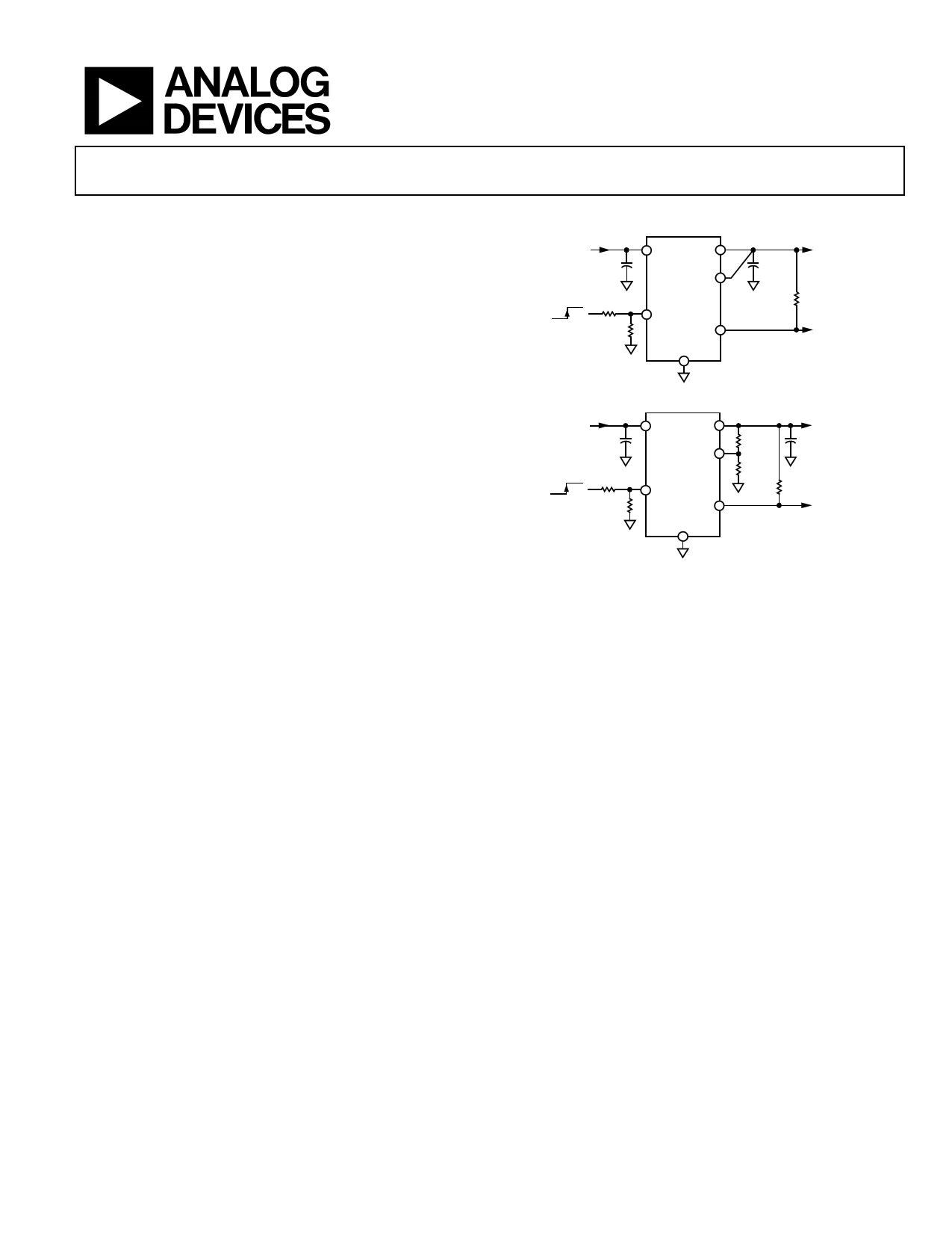
TYPICAL APPLICATION CIRCUITS
VIN = 8V
CIN +
1µF
ON
OFF
R1
100kΩ
R2
100kΩ
VIN VOUT
SENSE
EN/
UVLO
PG
GND
+ COUT
1µF
VOUT = 5V
RPG
100kΩ
PG
Figure 1. ADP7102 with Fixed Output Voltage, 5 V
VIN = 8V
CIN +
1µF
ON
OFF
R3
100kΩ
R4
100kΩ
VIN VOUT
ADJ
EN/
UVLO
PG
GND
R1
40.2kΩ
VOUT = 5V
+ COUT
1µF
R2
13kΩ
RPG
100kΩ
PG
Figure 2. ADP7102 with Adjustable Output Voltage, 5 V
The ADP7102 output noise voltage is 15 μV rms and is inde-
pendent of the output voltage. A digital power good output
allows power system monitors to check the health of the output
voltage. A user programmable precision undervoltage lockout
function facilitates sequencing of multiple power supplies.
The ADP7102 is available in 8-lead, 3 mm × 3 mm LFCSP
and 8-lead SOIC packages. The LFCSP offers a very compact
solution and also provides excellent thermal performance for
applications requiring up to 300 mA of output current in a
small, low-profile footprint.
Rev. A
Information furnished by Analog Devices is believed to be accurate and reliable. However, no
responsibilityisassumedbyAnalogDevices for itsuse,nor foranyinfringementsofpatentsor other
rights of third parties that may result from its use. Specifications subject to change without notice. No
license is granted by implication or otherwise under any patent or patent rights of Analog Devices.
Trademarksandregisteredtrademarksarethepropertyoftheirrespectiveowners.
One Technology Way, P.O. Box 9106, Norwood, MA 02062-9106, U.S.A.
Tel: 781.329.4700
www.analog.com
Fax: 781.461.3113
©2011 Analog Devices, Inc. All rights reserved.
Free Datasheet http://www.Datasheet4U.com
1 page 
Data Sheet
ABSOLUTE MAXIMUM RATINGS
Table 3.
Parameter
VIN to GND
VOUT to GND
EN/UVLO to GND
PG to GND
SENSE/ADJ to GND
Storage Temperature Range
Operating Junction Temperature Range
Operating Ambient Temperature Range
Soldering Conditions
Rating
–0.3 V to +22 V
–0.3 V to +20 V
–0.3 V to VIN
–0.3 V to VIN
–0.3 V to VOUT
–65°C to +150°C
–40°C to +125°C
–40°C to +85°C
JEDEC J-STD-020
Stresses above those listed under absolute maximum ratings
may cause permanent damage to the device. This is a stress
rating only and functional operation of the device at these or
any other conditions above those indicated in the operational
section of this specification is not implied. Exposure to absolute
maximum rating conditions for extended periods may affect
device reliability.
THERMAL DATA
Absolute maximum ratings apply individually only, not in
combination. The ADP7102 can be damaged when the junction
temperature limit is exceeded. Monitoring ambient temperature
does not guarantee that TJ is within the specified temperature
limits. In applications with high power dissipation and poor
thermal resistance, the maximum ambient temperature may
have to be derated.
In applications with moderate power dissipation and low PCB
thermal resistance, the maximum ambient temperature can
exceed the maximum limit as long as the junction temperature
is within specification limits. The junction temperature (TJ) of
the device is dependent on the ambient temperature (TA), the
power dissipation of the device (PD), and the junction-to-
ambient thermal resistance of the package (θJA).
Maximum junction temperature (TJ) is calculated from the
ambient temperature (TA) and power dissipation (PD) using the
formula
TJ = TA + (PD × θJA)
Junction-to-ambient thermal resistance (θJA) of the package is
based on modeling and calculation using a 4-layer board. The
junction-to-ambient thermal resistance is highly dependent on
the application and board layout. In applications where high
maximum power dissipation exists, close attention to thermal
ADP7102
board design is required. The value of θJA may vary, depending
on PCB material, layout, and environmental conditions. The
specified values of θJA are based on a 4-layer, 4 in. × 3 in. circuit
board. See JESD51-7 and JESD51-9 for detailed information on
the board construction. For additional information, see the
AN-617 Application Note, MicroCSP™ Wafer Level Chip Scale
Package, available at www.analog.com.
ΨJB is the junction-to-board thermal characterization parameter
with units of °C/W. The package’s ΨJB is based on modeling and
calculation using a 4-layer board. The JESD51-12, Guidelines
for Reporting and Using Electronic Package Thermal
Information, states that thermal characterization parameters are
not the same as thermal resistances. ΨJB measures the
component power flowing through multiple thermal paths
rather than a single path as in thermal resistance, θJB. Therefore,
ΨJB thermal paths include convection from the top of the
package as well as radiation from the package, factors that make
ΨJB more useful in real-world applications. Maximum junction
temperature (TJ) is calculated from the board temperature (TB)
and power dissipation (PD) using the formula
TJ = TB + (PD × ΨJB)
See JESD51-8 and JESD51-12 for more detailed information
about ΨJB.
Thermal Resistance
θJA and ΨJB are specified for the worst-case conditions, that is, a
device soldered in a circuit board for surface-mount packages.
θJC is a parameter for surface-mount packages with top
mounted heatsinks. θJC is presented here for reference only.
Table 4. Thermal Resistance
Package Type
θJA θJC ΨJB Unit
8-Lead LFCSP
40.1 27.1 17.2 °C/W
8-Lead SOIC
48.5 58.4 31.3 °C/W
ESD CAUTION
Rev. A | Page 5 of 28
Free Datasheet http://www.Datasheet4U.com
5 Page 
Data Sheet
1200
1000
800
LOAD = 100µA
LOAD = 1mA
LOAD = 10mA
LOAD = 100mA
LOAD = 300mA
600
400
200
0
2 4 6 8 10 12 14 16 18 20
VIN (V)
Figure 29. Ground Current vs. Input Voltage, VOUT = 1.8 V
5.08
LOAD = 100µA
5.07
LOAD = 1mA
LOAD = 10mA
LOAD = 100mA
5.06 LOAD = 300mA
5.05
5.04
5.03
5.02
5.01
5.00
4.99
4.98
–40°C
–5°C
25°C
TJ (°C)
85°C
125°C
Figure 30. Output Voltage vs. Junction Temperature, VOUT = 5 V, Adjustable
5.08
5.07
5.06
5.05
5.04
5.03
5.02
5.01
5.00
4.99
4.98
0.1
1 10 100
ILOAD (mA)
1000
Figure 31. Output Voltage vs. Load Current, VOUT = 5 V, Adjustable
ADP7102
5.08
LOAD = 100µA
5.07
LOAD = 1mA
LOAD = 10mA
LOAD = 100mA
5.06 LOAD = 300mA
5.05
5.04
5.03
5.02
5.01
5.00
4.99
4.98
6
8 10 12 14 16 18 20
VIN (V)
Figure 32. Output Voltage vs. Input Voltage, VOUT = 5 V, Adjustable
2.0
3.3V
4V
5V
6V
8V
1.5 10V
12V
15V
18V
20V
1.0
0.5
0
–40 –20
0
20 40 60 80 100 120 140
TEMPERATURE (°C)
Figure 33. Reverse Input Current vs. Temperature, VIN = 0 V, Different
Voltages on VOUT
0
LOAD = 300mA
–10
LOAD = 100mA
LOAD = 10mA
LOAD = 1mA
–20
–30
–40
–50
–60
–70
–80
–90
–100
10 100 1k 10k 100k 1M 10M
FREQUENCY (Hz)
Figure 34. Power Supply Rejection Ratio vs. Frequency, VOUT = 1.8 V,
VIN = 3.3 V
Rev. A | Page 11 of 28
Free Datasheet http://www.Datasheet4U.com
11 Page | ||
| Páginas | Total 28 Páginas | |
| PDF Descargar | [ Datasheet ADP7102.PDF ] | |
Hoja de datos destacado
| Número de pieza | Descripción | Fabricantes |
| ADP7102 | CMOS LDO | Analog Devices |
| ADP7104 | CMOS LDO | Analog Devices |
| ADP7105 | Low Noise LDO Regulator | Analog Devices |
| Número de pieza | Descripción | Fabricantes |
| SLA6805M | High Voltage 3 phase Motor Driver IC. |
Sanken |
| SDC1742 | 12- and 14-Bit Hybrid Synchro / Resolver-to-Digital Converters. |
Analog Devices |
|
DataSheet.es es una pagina web que funciona como un repositorio de manuales o hoja de datos de muchos de los productos más populares, |
| DataSheet.es | 2020 | Privacy Policy | Contacto | Buscar |