|
|
PDF P89C51RC2 Data sheet ( Hoja de datos )
| Número de pieza | P89C51RC2 | |
| Descripción | 8-bit Flash microcontroller | |
| Fabricantes | Philips | |
| Logotipo |  |
|
Hay una vista previa y un enlace de descarga de P89C51RC2 (archivo pdf) en la parte inferior de esta página. Total 30 Páginas | ||
|
No Preview Available !
INTEGRATED CIRCUITS
P89C51RA2xx/RB2xx/RC2xx/RD2xx
80C51 8-bit Flash microcontroller family
8KB/16KB/32KB/64KB ISP/IAP Flash with
512B/512B/512B/1KB RAM
Preliminary data
Supersedes data of 2002 May 20
2002 Jul 18
Philips
Semiconductors
http://www.Datasheet4U.com/
1 page 
Philips Semiconductors
80C51 8-bit Flash microcontroller family
8KB/16KB/32KB/64KB ISP/IAP Flash with 512B/512B/512B/1KB RAM
Preliminary data
P89C51RA2/RB2/RC2/RD2xx
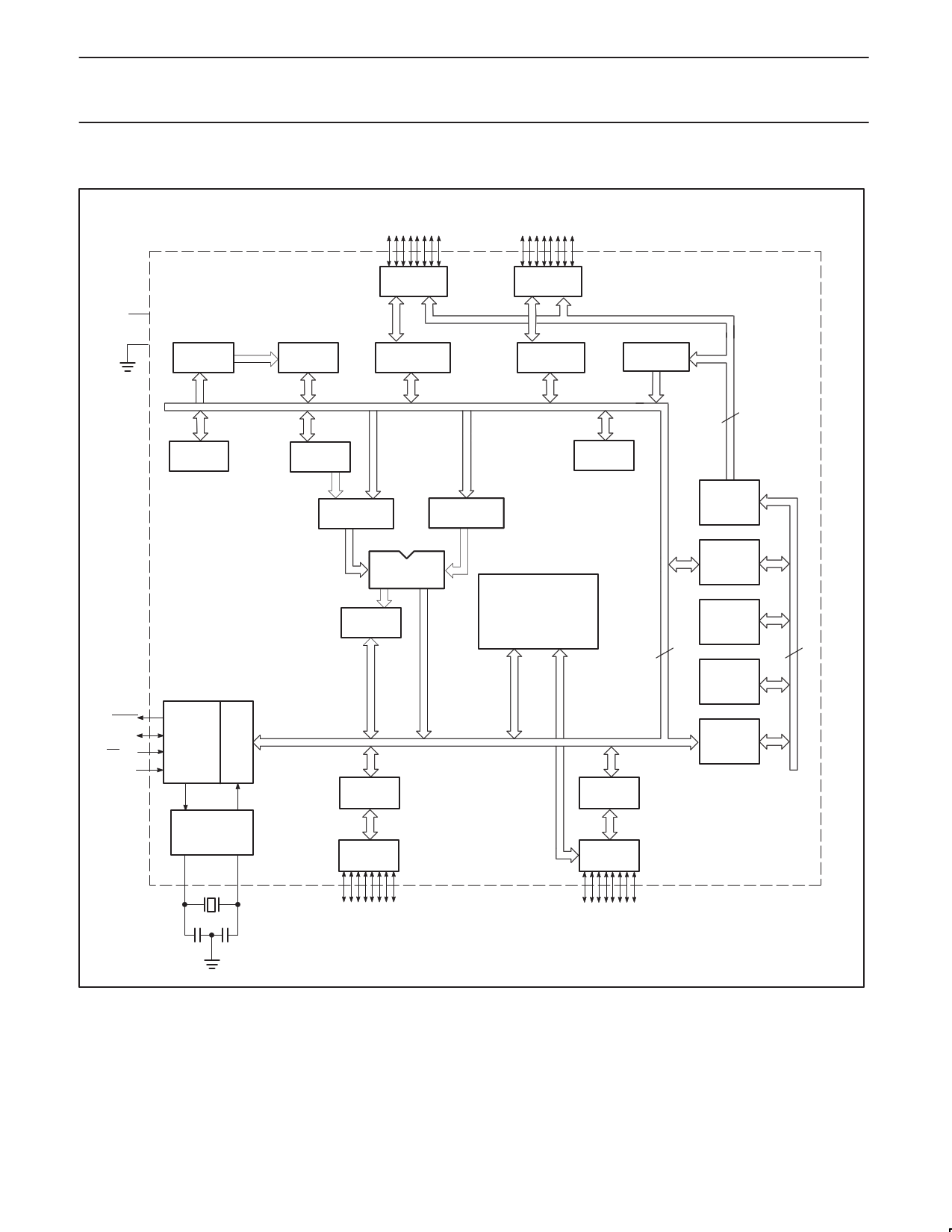
BLOCK DIAGRAM – CPU ORIENTED
P0.0–P0.7
VCC
VSS
RAM ADDR
REGISTER
RAM
PORT 0
DRIVERS
PORT 0
LATCH
P2.0–P2.7
PORT 2
DRIVERS
PORT 2
LATCH
FLASH
B
REGISTER
ACC
TMP2
TMP1
STACK
POINTER
8
PROGRAM
ADDRESS
REGISTER
ALU
PSW
PSEN
ALE
EAVPP
RST
TIMING
AND
CONTROL
PD
OSCILLATOR
XTAL1
XTAL2
PORT 1
LATCH
PORT 1
DRIVERS
P1.0–P1.7
SFRs
TIMERS
P.C.A.
PORT 3
LATCH
BUFFER
PC
INCRE-
MENTER
8
PROGRAM
COUNTER
DPTR’S
MULTIPLE
PORT 3
DRIVERS
P3.0–P3.7
16
SU01065
2002 Jul 18
5
http://www.Datasheet4U.com/
5 Page 
Philips Semiconductors
80C51 8-bit Flash microcontroller family
8KB/16KB/32KB/64KB ISP/IAP Flash with 512B/512B/512B/1KB RAM
Preliminary data
P89C51RA2/RB2/RC2/RD2xx
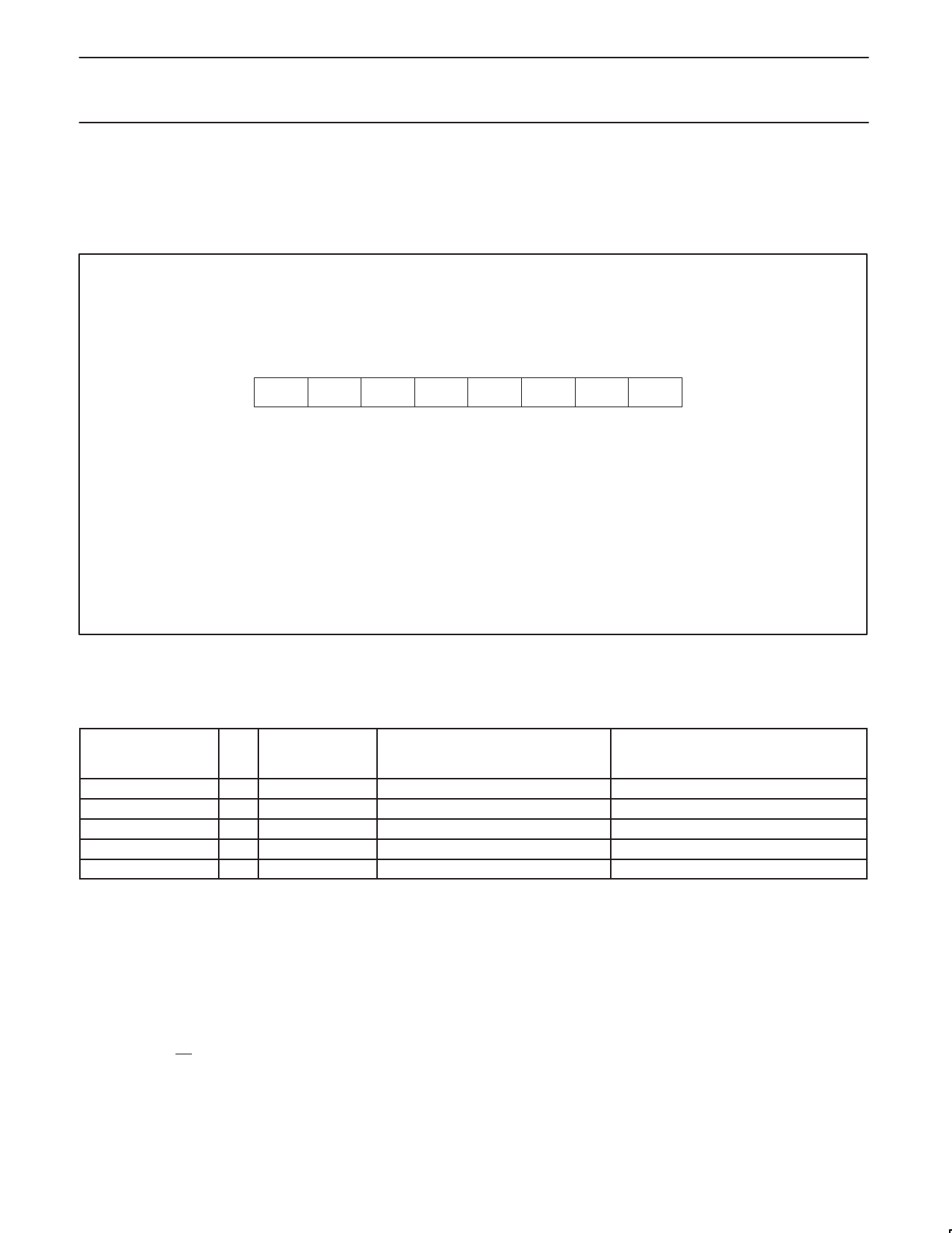
CLOCK CONTROL REGISTER (CKCON)
This device provides control of the 6-clock/12-clock mode by means
of both an SFR bit (X2) and a Flash bit (FX2, located in the Security
Block). The Flash clock control bit, FX2, when programmed (6-clock
mode) supercedes the X2 bit (CKCON.0).
The CKCON register also provides individual control of the clock
rates for the peripherals devices. When running in 6-clock mode
each peripheral may be individually clocked from either fosc/6 or
fosc/12. When in 12-clock mode, all peripheral devices will use
fosc/12. The CKCON register is shown below.
CKCON Address = 8Fh
Not Bit Addressable
Reset Value = x0000000B
76 54 321
– WDX2 PCAX2 SIX2 T2X2 T1X2 T0X2
0
X2
BIT
CKCON.7
CKCON.6
CKCON.5
CKCON.4
CKCON.3
CKCON.2
CKCON.1
CKCON.0
SYMBOL
–
WDX2
PCAX2
SIX2
T2X2
T1X2
T0X2
X2
FUNCTION
Reserved.
Watchdog clock; 0 = 6 clocks for each WDT clock, 1 = 12 clocks for each WDT clock
PCA clock; 0 = 6 clocks for each PCA clock, 1 = 12 clocks for each PCA clock
UART clock; 0 = 6 clocks for each UART clock, 1 = 12 clocks for each UART clock
Timer2 clock; 0 = 6 clocks for each Timer2 clock, 1 = 12 clocks for each Timer2 clock
Timer1 clock; 0 = 6 clocks for each Timer1 clock, 1 = 12 clocks for each Timer1 clock
Timer0 clock; 0 = 6 clocks for each Timer0 clock, 1 = 12 clocks for each Timer0 clock
CPU clock; 1 = 6 clocks for each machine cycle, 0 = 12 clocks for each machine cycle
SU01607
Bits 1 through 6 only apply if 6 clocks per machine cycle is chosen
(i.e.– Bit 0 = 1). If Bit 0 = 0 (12 clocks per machine cycle) then all
peripherals will have 12 clocks per machine cycle as their clock
source.
Also please note that the clock divider applies to the serial port for
modes 0 & 2 (fixed baud rate modes). This is because modes 1 & 3
(variable baud rate modes) use either Timer 1 or Timer 2.
Below is the truth table for the peripheral input clock sources.
FX2 clock mode bit X2 Peripheral clock
mode bit
(e.g., T0X2)
erased
0
x
erased
1
0
erased
1
1
programmed
x
0
programmed
x
1
CPU MODE
12-clock (default)
6-clock
6-clock
6-clock
6-clock
RESET
A reset is accomplished by holding the RST pin high for at least two
machine cycles (12 oscillator periods in 6-clock mode, or 24 oscillator
periods in 12-clock mode), while the oscillator is running. To ensure a
good power-on reset, the RST pin must be high long enough to allow
the oscillator time to start up (normally a few milliseconds) plus two
machine cycles. At power-on, the voltage on VCC and RST must
come up at the same time for a proper start-up. Ports 1, 2, and 3 will
asynchronously be driven to their reset condition when a voltage
above VIH1 (min.) is applied to RST.
The value on the EA pin is latched when RST is deasserted and has
no further effect.
Peripheral Clock Rate
12-clock (default)
6-clock
12-clock
6-clock
12-clock
2002 Jul 18
11
http://www.Datasheet4U.com/
11 Page | ||
| Páginas | Total 30 Páginas | |
| PDF Descargar | [ Datasheet P89C51RC2.PDF ] | |
Hoja de datos destacado
| Número de pieza | Descripción | Fabricantes |
| P89C51RC+ | 80C51 8-bit Flash microcontroller family 32K/64K ISP FLASH with 512.1K RAM | NXP Semiconductors |
| P89C51RC+IA | 80C51 8-bit Flash microcontroller family 32K/64K ISP FLASH with 512.1K RAM | NXP Semiconductors |
| P89C51RC+IB | 80C51 8-bit Flash microcontroller family 32K/64K ISP FLASH with 512.1K RAM | NXP Semiconductors |
| P89C51RC+IN | 80C51 8-bit Flash microcontroller family 32K/64K ISP FLASH with 512.1K RAM | NXP Semiconductors |
| Número de pieza | Descripción | Fabricantes |
| SLA6805M | High Voltage 3 phase Motor Driver IC. |
Sanken |
| SDC1742 | 12- and 14-Bit Hybrid Synchro / Resolver-to-Digital Converters. |
Analog Devices |
|
DataSheet.es es una pagina web que funciona como un repositorio de manuales o hoja de datos de muchos de los productos más populares, |
| DataSheet.es | 2020 | Privacy Policy | Contacto | Buscar |
