|
|
PDF AT25DQ161 Data sheet ( Hoja de datos )
| Número de pieza | AT25DQ161 | |
| Descripción | 16-Megabit 2.7-volt Minimum SPI Serial Flash Memory | |
| Fabricantes | Atmel Corporation | |
| Logotipo |  |
|
Hay una vista previa y un enlace de descarga de AT25DQ161 (archivo pdf) en la parte inferior de esta página. Total 30 Páginas | ||
|
No Preview Available !
Features
• Single 2.7V - 3.6V Supply
• Serial Peripheral Interface (SPI) Compatible
– Supports SPI Modes 0 and 3
– Supports RapidS Operation
– Supports Dual- and Quad-Input Program
– Supports Dual- and Quad-Output Read
• Very High Operating Frequencies
– 100 MHz for RapidS
– 85 MHz for SPI
– Clock-to-Output (tV) of 5 ns Maximum
• Flexible, Optimized Erase Architecture for Code + Data Storage Applications
– Uniform 4-Kbyte Block Erase
– Uniform 32-Kbyte Block Erase
– Uniform 64-Kbyte Block Erase
– Full Chip Erase
• Individual Sector Protection with Global Protect/Unprotect Feature
– 32 Sectors of 64-Kbytes Each
• Hardware Controlled Locking of Protected Sectors via WP Pin
• Sector Lockdown
– Make Any Combination of 64-Kbyte Sectors Permanently Read-Only
• 128-Byte Programmable OTP Security Register
• Flexible Programming
– Byte/Page Program (1 to 256 Bytes)
• Fast Program and Erase Times
– 1.0 ms Typical Page Program (256 Bytes) Time
– 50 ms Typical 4-Kbyte Block Erase Time
– 250 ms Typical 32-Kbyte Block Erase Time
– 400 ms Typical 64-Kbyte Block Erase Time
• Program and Erase Suspend/Resume
• Automatic Checking and Reporting of Erase/Program Failures
• Software Controlled Reset
• JEDEC Standard Manufacturer and Device ID Read Methodology
• Low Power Dissipation
– 5 mA Active Read Current (Typical at 20 MHz)
– 5 µA Deep Power-Down Current (Typical)
• Endurance: 100,000 Program/Erase Cycles
• Data Retention: 20 Years
• Complies with Full Industrial Temperature Range
• Industry Standard Green (Pb/Halide-free/RoHS Compliant) Package Options
– 8-lead SOIC (150-mil and 208-mil wide)
– 8-pad Ultra Thin DFN (5 x 6 x 0.6 mm)
16-Megabit
2.7-volt
Minimum
SPI Serial Flash
Memory with
Dual-I/O and
Quad-I/O
Support
AT25DQ161
Preliminary
8671A–DFLASH–07/09
http://www.Datasheet4U.com
1 page 
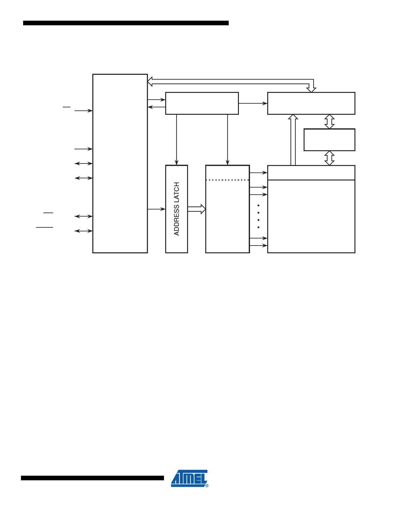
3. Block Diagram
Figure 3-1. Block Diagram
AT25DQ161 [Preliminary]
CONTROL AND
CS PROTECTION LOGIC
SCK
SI (I/O0)
SO (I/O1)
INTERFACE
CONTROL
AND
LOGIC
WP (I/O2)
HOLD (I/O3)
Y-DECODER
X-DECODER
I/O BUFFERS
AND LATCHES
SRAM
DATA BUFFER
Y-GATING
FLASH
MEMORY
ARRAY
Note: I/O3-0 pin naming convention is used for Dual-I/O and Quad-I/O commands
4. Memory Array
To provide the greatest flexibility, the memory array of the AT25DQ161 can be erased in four
levels of granularity including a full chip erase. In addition, the array has been divided into phys-
ical sectors of uniform size, of which each sector can be individually protected from program and
erase operations. The size of the physical sectors is op timized for both code and data storage
applications, allowing both code and data segments to reside in their own isolated regions. The
Memory Architecture Diagram illustrates the breakdown of each erase level as well a s the
breakdown of each physical sector.
8671A–DFLASH–07/09
5
5 Page 
AT25DQ161 [Preliminary]
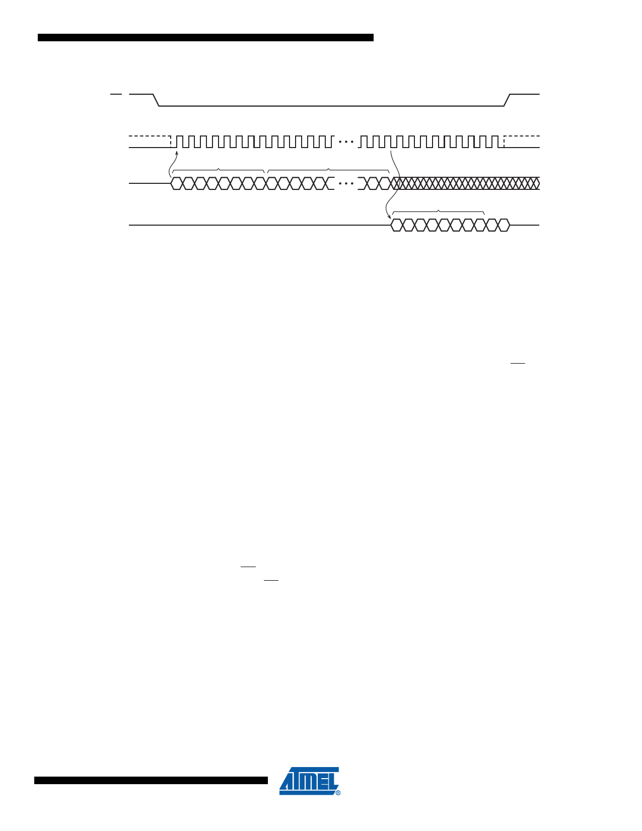
Figure 7-3. Read Array – 03h Opcode
CS
SCK
SI
SO
0 1 2 3 41 5 67
81 9 0 11 2
29 30 31 32 33 34 35 36 37 38 39 40
OPCODE
00000011
MSB
HIGH-IMPEDANCE
ADDRESS BITS A23-A0
AAAAAA
MSB
AAA
DATA BYTE 1
DDDDDDDDDD
MSB
MSB
7.2 Dual-Output Read Array
The Dual-Output Read Array command is similar to the standard Read Array command and can
be used to sequentially read a continuous stream of data from the device by simply providing the
clock signal once the initial starting address has been specified. Unlike the standard Read Array
command, however, the Dual-Output Read Array command allows two bits of data to be clocked
out of the device on every clock cycle rather than just one.
The Dual-Output Read Array command can be used at any clock frequency up to the maximum
specified by fRDDO. To perform the Dual-Output Read Array operation, the CS pin must first be
asserted and the opcode of 3Bh must be clocked into the device. After the opcode has been
clocked in, the three address bytes must be clocked in to specify the starting address location of
the first byte to read within the memory array. Following the three address bytes, a single
dummy byte must also be clocked into the device.
After the three address bytes and the dummy byte have been clocked in, additional clock cycles
will result in data being output on both the I/O1 and I/O0 pins. The data is always output with the
MSB of a byte first, and the MSB is always output on the I/O1 pin. During the first clock cycle, bit
7 of the first data byte will be output on the I/O1 pin while bit 6 of the same data byte will be out-
put on the I/O0 pin. During the next clock cycle, bits 5 and 4 of the first data byte will be output on
the I/O1 and I/O0 pins, respectively. The sequence continues with each byte of data being output
after every four clock cycles. When the last byte (1FFFFFh) of the memory array has been read,
the device will continue reading back at the beginning of the array (000000h). No delays will be
incurred when wrapping around from the end of the array to the beginning of the array.
Deasserting the CS pin will terminate the read operation and put the I/O1-0 pins into a high-
impedance state. The CS pin can be deasserted at any time and does not require that a full byte
of data be read.
8671A–DFLASH–07/09
11
11 Page | ||
| Páginas | Total 30 Páginas | |
| PDF Descargar | [ Datasheet AT25DQ161.PDF ] | |
Hoja de datos destacado
| Número de pieza | Descripción | Fabricantes |
| AT25DQ161 | 16-Megabit 2.7-volt Minimum SPI Serial Flash Memory | Atmel Corporation |
| Número de pieza | Descripción | Fabricantes |
| SLA6805M | High Voltage 3 phase Motor Driver IC. |
Sanken |
| SDC1742 | 12- and 14-Bit Hybrid Synchro / Resolver-to-Digital Converters. |
Analog Devices |
|
DataSheet.es es una pagina web que funciona como un repositorio de manuales o hoja de datos de muchos de los productos más populares, |
| DataSheet.es | 2020 | Privacy Policy | Contacto | Buscar |
