|
|
|
PDF LM4940 Data sheet ( Hoja de datos )
| Número de pieza | LM4940 | |
| Descripción | 6W Stereo Audio Power Amplifier | |
| Fabricantes | National Semiconductor | |
| Logotipo | ||
Hay una vista previa y un enlace de descarga de LM4940 (archivo pdf) en la parte inferior de esta página. Total 14 Páginas | ||
|
No Preview Available !
October 2003
LM4940
6W Stereo Audio Power Amplifier
General Description
The LM4940 is a dual audio power amplifier primarily de-
signed for demanding applications in flat panel monitors and
TV’s. It is capable of delivering 6 watts per channel to a 4Ω
load with less than 10% THD+N while operating on a
14.4VDC power supply.
Boomer audio power amplifiers were designed specifically to
provide high quality output power with a minimal amount of
external components. The LM4940 does not require boot-
strap capacitors or snubber circuits. Therefore, it is ideally
suited for display applications requiring high power and mini-
mal size.
The LM4940 features a low-power consumption active-low
shutdown mode. Additionally, the LM4940 features an inter-
nal thermal shutdown protection mechanism along with short
circuit protection.
The LM4940 contains advanced pop & click circuitry that
eliminates noises which would otherwise occur during
turn-on and turn-off transitions.
The LM4940 is a unity-gain stable and can be configured by
external gain-setting resistors.
Key Specifications
j Quiscent Power Supply Current
j POUT (SE)
VDD = 14.4V, RL = 4Ω, 10% THD+N
j Shutdown current
40mA (max)
6W (typ)
40µA (typ)
Features
n Pop & click circuitry eliminates noise during turn-on and
turn-off transitions
n Low current, active-low shutdown mode
n Low quiescent current
n Stereo 6W output, RL = 4Ω
n Short circuit protection
n Unity-gain stable
n External gain configuration capability
Applications
n Flat Panel Monitors
n Flat Panel TV’s
n Computer Sound Cards
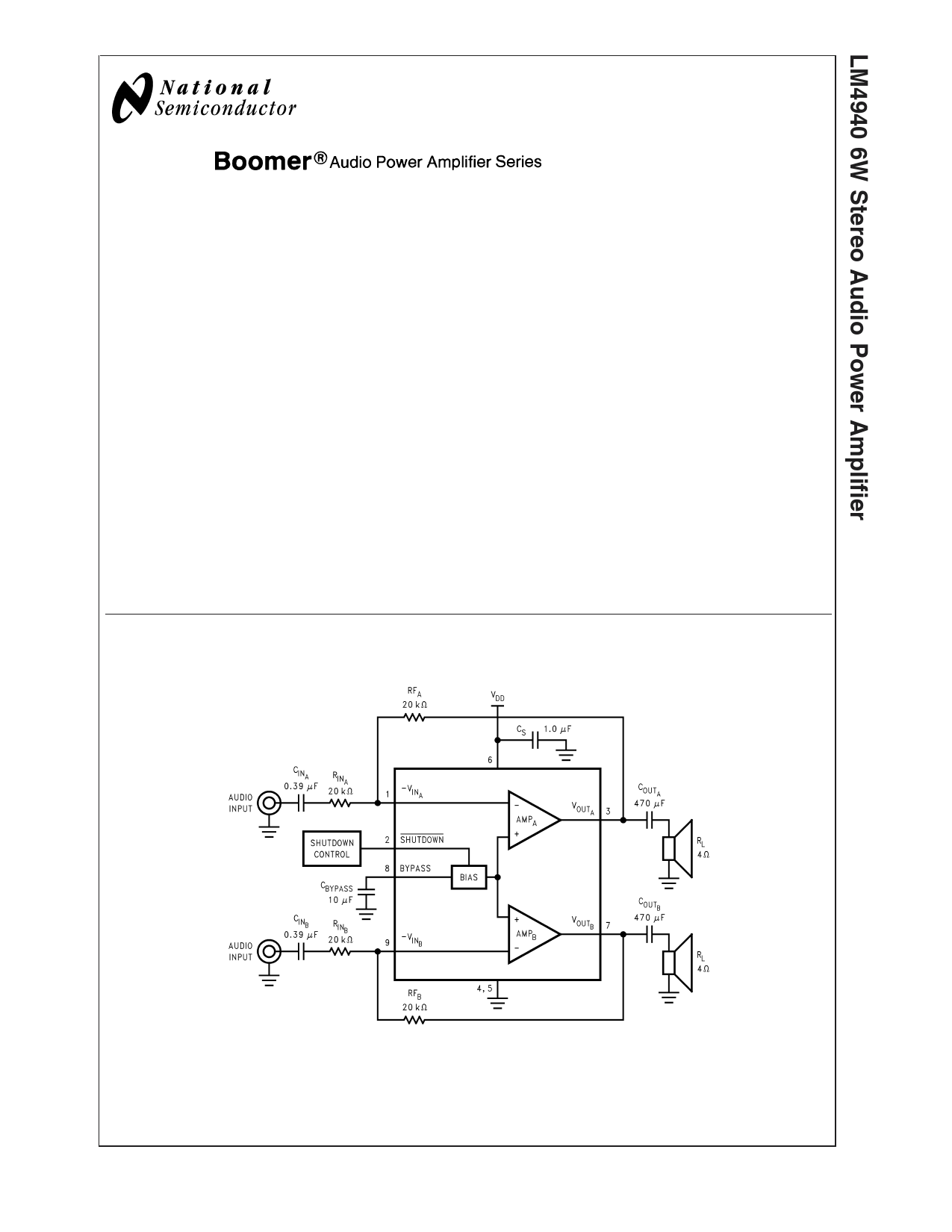
Typical Application
20075672
FIGURE 1. Typical Stereo Audio Amplifier Application Circuit
Boomer® is a registered trademark of National Semiconductor Corporation.
© 2003 National Semiconductor Corporation DS200756
www.national.com
http://www.Datasheet4U.com
1 page 
Typical Performance Characteristics
THD+N vs Frequency
THD+N vs Frequency
20075699
VDD = 12V, RL = 4Ω, SE operation,
both channels driven and loaded (average shown),
POUT = 1W, AV = 1
THD+N vs Frequency
200756A0
VDD = 12V, RL = 4Ω, SE operation,
both channels driven and loaded (average shown),
POUT = 2.5W, AV = 1
THD+N vs Output Power
200756A1
VDD = 12V, RL = 8Ω, SE operation,
both channels driven and loaded (average shown),
POUT = 1W, AV = 1
THD+N vs Output Power
200756F3
VDD = 14.4V, RL = 4Ω, SE operation, AV = 1
single channel driven/single channel measured,
fIN = 1kHz
THD+N vs Output Power
200756D9
VDD = 12V, RL = 4Ω, SE operation, AV = 1
single channel driven/single channel measured,
fIN = 1kHz
200756E0
VDD = 12V, RL = 8Ω, SE operation, AV = 1
single channel driven/single channel measured,
fIN = 1kHz
5 www.national.com
5 Page 
Application Information (Continued)
CB (µF)
1.0
2.2
4.7
10
TON (ms)
120
120
200
440
In order eliminate "clicks and pops", all capacitors must be
discharged before turn-on. Rapidly switching VDD may not
allow the capacitors to fully discharge, which may cause
"clicks and pops".
There is a relationship between the value of CIN and
CBYPASS that ensures minimum output transient when power
is applied or the shutdown mode is deactivated. Best perfor-
mance is achieved by setting the time constant created by
CIN and Ri + Rf to a value less than the turn-on time for a
given value of CBYPASS as shown in the table above.
AUDIO POWER AMPLIFIER DESIGN
Audio Amplifier Design: Driving 3W into a 4Ω load
The following are the desired operational parameters:
Power Output
Load Impedance
3WRMS
4Ω
Input Level
Input Impedance
0.3VRMS (max)
20kΩ
Bandwidth
100Hz–20kHz ± 0.25dB
The design begins by specifying the minimum supply voltage
necessary to obtain the specified output power. One way to
find the minimum supply voltage is to use the Output Power
vs Power Supply Voltage curve in the Typical Performance
Characteristics section. Another way, using Equation (8), is
to calculate the peak output voltage necessary to achieve
the desired output power for a given load impedance. To
account for the amplifier’s dropout voltage, two additional
voltages, based on the Clipping Dropout Voltage vs Power
Supply Voltage in the Typical Performance Characteris-
tics curves, must be added to the result obtained by Equa-
tion (8). The result is Equation (9).
(6)
VDD = VOUTPEAK + VODTOP + VODBOT
(7)
The Output Power vs. Power Supply Voltage graph for an 8Ω
load indicates a minimum supply voltage of 11.8V. The com-
monly used 12V supply voltage easily meets this. The addi-
tional voltage creates the benefit of headroom, allowing the
LM4940 to produce an output power of 3W without clipping
or other audible distortion. The choice of supply voltage must
also not create a situation that violates of maximum power
dissipation as explained above in the Power Dissipation
section. After satisfying the LM4940’s power dissipation re-
quirements, the minimum differential gain needed to achieve
3W dissipation in a 4Ω BTL load is found using Equation
(10).
(8)
Thus, a minimum gain of 11.6 allows the LM4940’s to reach
full output swing and maintain low noise and THD+N perfor-
mance. For this example, let AV = 12. The amplifier’s overall
BTL gain is set using the input (RINA) and feedback (R)
resistors of the first amplifier in the series BTL configuration.
Additionaly, AV-BTL is twice the gain set by the first amplifier’s
RIN and Rf. With the desired input impedance set at 20kΩ,
the feedback resistor is found using Equation (11).
Rf / RIN =A V
(9)
The value of Rf is 240kΩ. The nominal output power is 3W.
The last step in this design example is setting the amplifier’s
-3dB frequency bandwidth. To achieve the desired ±0.25dB
pass band magnitude variation limit, the low frequency re-
sponse must extend to at least one-fifth the lower bandwidth
limit and the high frequency response must extend to at least
five times the upper bandwidth limit. The gain variation for
both response limits is 0.17dB, well within the ±0.25dB-
desired limit. The results are an
and an
fL = 100Hz/5= 20Hz
(10)
fL = 20kHzx5= 100kHz
(11)
As mentioned in the SELECTING EXTERNAL COMPO-
NENTS section, RINA and CINA, as well as COUT and RL,
create a highpass filter that sets the amplifier’s lower band-
pass frequency limit. Find the coupling capacitor’s value
using Equation (14).
The result is
CIN =1 / 2πRINfL
(12)
1 / (2πx20kΩx20Hz) = 0.398µF = CIN
and
1
/
(2πx4Ωx20Hz)
=
1989µF
=
C
OUT
Use a 0.39µF capacitor for CIN and a 2000µF capacitor for
COUT, the closest standard values.
The product of the desired high frequency cutoff (100kHz in
this example) and the differential gain AV, determines the
upper passband response limit. With AV = 12 and fH =
100kHz, the closed-loop gain bandwidth product (GBWP) is
1.2mHz. This is less than the LM4940’s 3.5MHz GBWP. With
this margin, the amplifier can be used in designs that require
more differential gain while avoiding performance restricting
bandwidth limitations.
11 www.national.com
11 Page | ||
| Páginas | Total 14 Páginas | |
| PDF Descargar | [ Datasheet LM4940.PDF ] | |
Hoja de datos destacado
| Número de pieza | Descripción | Fabricantes |
| LM494 | Pulse Width Modulated Control Circuit | National Semiconductor |
| LM4940 | LM4940 6W Stereo Audio Power Amplifier (Rev. C) | Texas Instruments |
| LM4940 | 6W Stereo Audio Power Amplifier | National Semiconductor |
| LM4940 | 6W Stereo Audio Power Amplifier | National Semiconductor |
| Número de pieza | Descripción | Fabricantes |
| SLA6805M | High Voltage 3 phase Motor Driver IC. |
Sanken |
| SDC1742 | 12- and 14-Bit Hybrid Synchro / Resolver-to-Digital Converters. |
Analog Devices |
|
DataSheet.es es una pagina web que funciona como un repositorio de manuales o hoja de datos de muchos de los productos más populares, |
| DataSheet.es | 2020 | Privacy Policy | Contacto | Buscar |