|
|
|
PDF NX2422 Data sheet ( Hoja de datos )
| Número de pieza | NX2422 | |
| Descripción | TWO PHASE SYNCHRONOUS PWM CONTROLLER | |
| Fabricantes | Microsemi | |
| Logotipo | ||
Hay una vista previa y un enlace de descarga de NX2422 (archivo pdf) en la parte inferior de esta página. Total 20 Páginas | ||
|
No Preview Available !
NX2422
TWO PHASE SYNCHRONOUS PWM CONTROLLER WITH
INTEGRATED FET DRIVER, DIFFERENTIAL CURRENT SENSE
& 5V BIAS REGULATOR
PRELIMINARY DATA SHEET Pb Free Product
DESCRIPTION
FEATURES
The NX2422 is a two-phase PWM controller with inte- n Differential inductor DCR sensing eliminates the
grated FET driver designed for low voltage high current problem with layout parasitic
application. The two phase synchronous buck converter n 5V bias regulator available
offers ripple cancelation for both input and output. The n Low Impedance On-board Drivers
NX2422 uses differential remote sensing using either cur-
rent sense resistor or inductor DCR sensing to achieve
accurate current matching between the two channels.
n
n
n
Hiccup current limit and IOUT indication
Power Good for power sequencing
EN2_B pin allows the slave channel on and off while
Differential sensing eliminates the error caused by PCB the master channel is working
board trace resistance that otherwise presents when us- n Programmable frequency
ing a single ended voltage sensing.
n Prebias start up
In addition the NX2422 offers high drive current capabil- n OVP without negative spike at output
ity especially for keeping the synchronous MOSFET off n Selectable between internal and external reference
during SW node transition, can provide regulated 5V to n Internal Schottky diode from PVCC to BST
IC biasing and drivers via 5V bias regulator, allows the n Pb-free and RoHS compliant
slave channel on and off via EN2_B pin while the main
APPLICATIONS
channel is working. Other features: PGOOD output, pro- n Graphic card High Current Vcore Supply
grammable switching frequency and hiccup current lim-n High Current on board DC to DC converter
iting circuitry.
applications
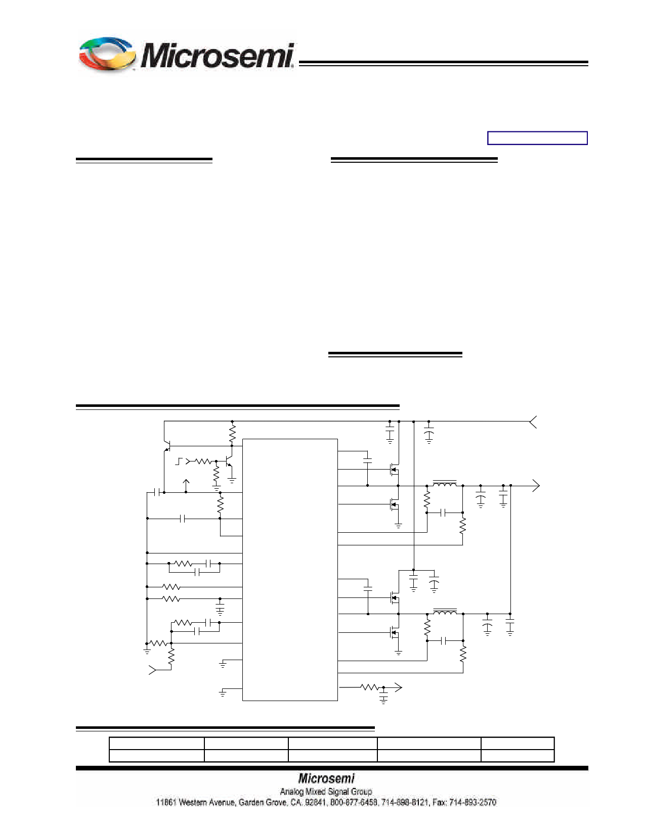
TYPICAL APPLICATION
2N3904
R10
2N3904
VCCDRV
BST1
R13
5V R14
C31
C30
R11
R15 C29
PVCC
5VCC
REFIN
AGND
CSCOMP
HDRV1
SW1
LDRV1
CS+1
CS-1
R16 C28
R17
R18 C26
R19 C25
R20
VOUT
RT
IOUT/IMAX
C27
VCOMP
FB
EN2_B
BST2
HDRV2
SW2
LDRV2
CS+2
CS-2
PGND(PAD) INREFOUT/POK
C11 C10
C12
Q1
Q2
L1
R29
C15
C13 C14
R28
C17 C18
C19
Q3
L2
R27
Q4 C22
C20 C21
R26
R24
C24
Ref for external circuitry
12V BUS
VOUT
Figure1 - Typical application of NX2422
ORDERING INFORMATION
Device
NX2422CMTR
Temperature
Package
0 to 70oC MLPQ 4x4 - 24L
Frequency
50kHz to 1MHz
Pb-Free
Yes
Rev.2.1
12/01/08
1
1 page 
NX2422
PIN DESCRIPTIONS
SYMBOL
PIN DESCRIPTION
HDRV1
High side gate driver for Channel 1.
BST1
Bootstrap supply for Channel 1.
5VCC
IC’s supply voltage. This pin biases the internal logic circuits. A minimum 1uF
ceramic capacitor is recommended to connect from this pin to ground plane.
AGND
Controller analog ground pin.
EN2_B
This pin is used to startup or shutdown the channel2 only while 5VCC and REFIN is
ready. For two phase opeartion, EN2_B is preferred to be tied to GND. For one
phase opeartion, EN2_B is preferred to be tied to 5VCC. During the operation, it is
not recommended to change EN2_B voltage.
CS+1
Positive input of the channel 1 differential current sense amplifiers. It is connected
directly to the RC junction of the respective phase’s output inductor.
CS-1
Negative input of the channel 1 differential current sense amplifiers. It is con-
nected directly to the negative side of the respective phase’s output inductor.
CS-2
Negative input of the channel 2 differential current sense amplifiers. It is con-
nected directly to the negative side of the respective phase’s output inductor.
CS+2
Positive input of the channel 2 differential current sense amplifiers. It is connected
directly to the RC junction of the respective phase’s output inductor.
IOUT/IMAX
This pin indicates average output current level and sets OCP threshold using a
resistor from this pin to ground. A no more than 1nF ceramic capacitor is recom-
mended to connect this pin to ground plane to filter the noise on this pin.
RT This pin programs the internal oscillator frequency using a resistor from this pin to
ground.
VCOMP
This is the output pin of the error amplifier.
FB This pin is the error amplifier inverting input. It is connected to the output voltage via
a voltage divider.
CSCOMP
The output of the transconductance op amp for current balance circuit. An
external RC is connected from this pin to GND to stabilize the current loop.
REFIN
External reference input. If pull-up to >4.5V, internal reference is used. If driven by
an external voltage ranged from 0.4V to 2.5V, external reference is used with slew
rate following SS rate. If REFIN is below 0.4V, device is disabled.
INREFOUT/
POK
This pin has dual functions. When FB pin is below 75% of internal 0.6V reference,
this pin is held low. When FB reaches above this threshold, this pin is tied to an
internal 1.25V reference, allowing it to be used as a reference for any external op
amp circuitry as well as an indicator of power OK. This pin can not be connected
directly to an output capacitor. An RC network is needed which also provides a slow
ramp up of the reference for the external op amp.
Rev.2.1
12/01/08
5
5 Page 
NX2422
two 1.5uH inductors.
1.Calculate the location of LC double pole FLC
and ESR zero FESR.
FLC = 2× π ×
1
LEFF × COUT
=1
2×π× 0.75uH×10800uF
= 1.768kHz
FESR
=
1
2 × π × ESR × COUT
=1
2 × π ×13mΩ ×1800uF
= 6.801kHz
2.Set R2 equal to10kΩ and calculate R1.
R1=
R2 ×
VOUT
VREF
-VREF
= 10kΩ × 0.6V
1.2V-0.6V
= 10kΩ
3. Set crossover frequency FO=15kHz.
4.Calculate R3 value by the following equation.
R3=
VOSC
Vin
×
2 × π × FO × L EFF
ESR
× R2
= 1V × 2 × π × 15kHz × 0.75uH × 10kΩ
12V
2.16m Ω
=27.3kΩ
Choose
R
3
=27.4kΩ.
5. Calculate C by setting compensator zero F
1Z
at 75% of the LC double pole.
1
C1= 2 × π ×R3 ×Fz
=1
2× π × 27.4kΩ× 0.75 ×1.768kHz
=4.4nF
Choose C =4.7nF.
1
6.
Calculate
C
2
by
setting
compensator
pole
Fp
at half the swithing frequency.
C2=
π
×
1
R3
×
Fs
=1
π × 27.4kΩ × 400kH z
=30pF
Choose C2=33pF.
Rev.2.1
12/01/08
B. Type III compensator design
For low ESR output capacitors, typically such as
Sanyo OSCON and POSCAP, the frequency of ESR zero
caused by output capacitors is higher than the cross-
over frequency. In this case, it is necessary to compen-
sate the system with type III compensator.
In design example, six electrolytic capacitors are
used as output capacitors. The system is compensated
with type III compensator. The following figures and equa-
tions show how to realize the this type III compensator
with electrolytic capacitors.
FZ1
=
2×
π
1
× R4
×
C2
FZ2
=
1
2 × π × (R2 + R3 ) × C3
FP1
=
2×
π
1
× R3
×
C3
FP2
=
1
2
×
π
×
R4
×
C1
C1
×
+
C2
C2
...(14)
...(15)
...(16)
...(17)
where FZ1,FZ2,FP1 and FP2 are poles and zeros in
the compensator.
Vout
Zin
R3
R2
C3
R1
Zf
C1
C2 R4
Fb
Vref
Ve
Figure 5 - Type III compensator
11
11 Page | ||
| Páginas | Total 20 Páginas | |
| PDF Descargar | [ Datasheet NX2422.PDF ] | |
Hoja de datos destacado
| Número de pieza | Descripción | Fabricantes |
| NX2422 | TWO PHASE SYNCHRONOUS PWM CONTROLLER | Microsemi |
| Número de pieza | Descripción | Fabricantes |
| SLA6805M | High Voltage 3 phase Motor Driver IC. |
Sanken |
| SDC1742 | 12- and 14-Bit Hybrid Synchro / Resolver-to-Digital Converters. |
Analog Devices |
|
DataSheet.es es una pagina web que funciona como un repositorio de manuales o hoja de datos de muchos de los productos más populares, |
| DataSheet.es | 2020 | Privacy Policy | Contacto | Buscar |