|
|
|
PDF MAX4193EPA Data sheet ( Hoja de datos )
| Número de pieza | MAX4193EPA | |
| Descripción | CMOS Micropower Step-Up Switching Regulator | |
| Fabricantes | Maxim Integrated | |
| Logotipo | ||
Hay una vista previa y un enlace de descarga de MAX4193EPA (archivo pdf) en la parte inferior de esta página. Total 14 Páginas | ||
|
No Preview Available !
19-0915; Rev 2; 9/08
CMOS Micropower Step-Up
Switching Regulator
General Description
Maxim’s MAX630 and MAX4193 CMOS DC-DC regula-
tors are designed for simple, efficient, minimum-size
DC-DC converter circuits in the 5mW to 5W range. The
MAX630 and MAX4193 provide all control and power
handling functions in a compact 8-pin package: a
1.31V bandgap reference, an oscillator, a voltage com-
parator, and a 375mA N-channel output MOSFET. A
comparator is also provided for low-battery detection.
Operating current is only 70µA and is nearly indepen-
dent of output switch current or duty cycle. A logic-level
input shuts down the regulator to less than 1µA quies-
cent current. Low-current operation ensures high effi-
ciency even in low-power battery-operated systems.
The MAX630 and MAX4193 are compatible with most
battery voltages, operating from 2.0V to 16.5V.
The devices are pin compatible with the Raytheon bipo-
lar circuits, RC4191/2/3, while providing significantly
improved efficiency and low-voltage operation. Maxim
also manufactures the MAX631, MAX632, and MAX633
DC-DC converters, which reduce the external compo-
nent count in fixed-output 5V, 12V, and 15V circuits.
See Table 2 at the end of this data sheet for a summary
of other Maxim DC-DC converters.
Applications
+5V to +15V DC-DC Converters
High-Efficiency Battery-Powered DC-DC
Converters
+3V to +5V DC-DC Converters
9V Battery Life Extension
Uninterruptible 5V Power Supplies
5mW to 5W Switch-Mode Power Supplies
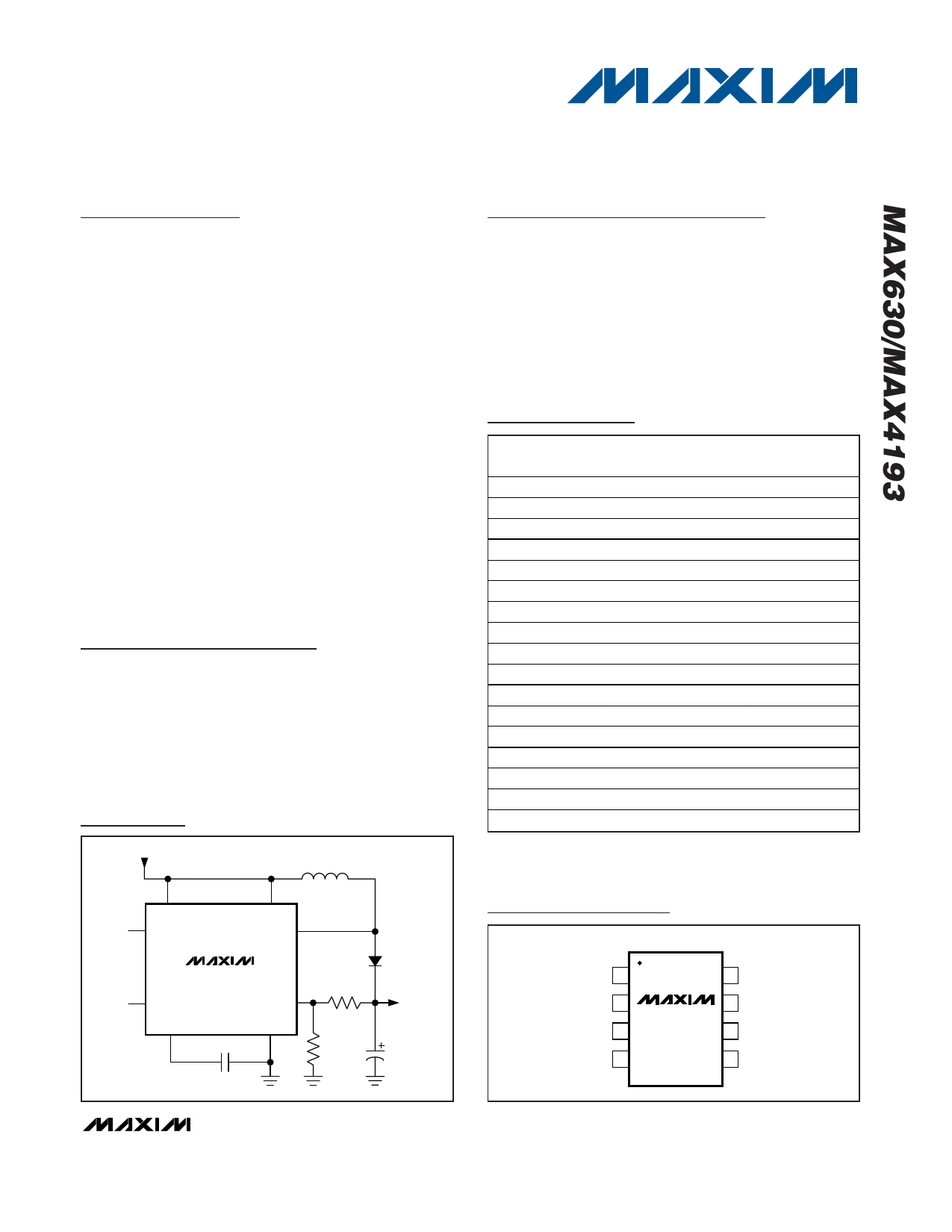
Typical Operating Circuit
+5V IN
470μH
6
IC
8 LBD
5
+VS
LX 3
1 LBR
CX
2
MAX630
47pF
VFB 7
GND
4
+5 TO +15V CONVERTER
+15V
OUT
Features
♦ High Efficiency—85% (typ)
♦ 70µA Typical Operating Current
♦ 1µA Maximum Quiescent Current
♦ 2.0V to 16.5V Operation
♦ 525mA (Peak) Onboard Drive Capability
♦ ±1.5% Output Voltage Accuracy (MAX630)
♦ Low-Battery Detector
♦ Compact 8-Pin Mini-DIP and SO Packages
♦ Pin Compatible with RC4191/2/3
Ordering Information
PART
TEMP RANGE
PIN-
PACKAGE
MAX630CPA
0°C to +70°C
8 PDIP
MAX630CSA
0°C to +70°C
8 SO
MAX630CJA
0°C to +70°C
8 CERDIP
MAX630EPA
-40°C to +85°C
8 PDIP
MAX630ESA
-40°C to +85°C
8 SO
MAX630EJA
-40°C to +85°C
8 CERDIP
MAX630MJA
-55°C to +125°C
8 CERDIP**
MAX630MSA/PR
-55°C to +125°C
8 SO†
MAX630MSA/PR-T -55°C to +125°C
8 SO†
MAX4193C/D
0°C to +70°C
Dice*
MAX4193CPA
0°C to +70°C
8 PDIP
MAX4193CSA
0°C to +70°C
8 SO
MAX4193CJA
0°C to +70°C
8 CERDIP
MAX4193EPA
-40°C to +85°C
8 PDIP
MAX4193ESA
-40°C to +85°C
8 SO
MAX4193EJA
-40°C to +85°C
8 CERDIP
MAX4193MJA
-55°C to +125°C
8 CERDIP**
*Dice are specified at TA = +25°C. Contact factory for dice
specifications.
**Contact factory for availability and processing to MIL-STD-883.
†Contact factory for availibility.
Pin Configuration
TOP VIEW
LBR 1
CX 2
LX 3
GND 4
MAX630
MAX4193
8 LBD
7 VFB
6 IC
5 +VS
________________________________________________________________ Maxim Integrated Products 1
For pricing, delivery, and ordering information, please contact Maxim/Dallas Direct! at
1-888-629-4642, or visit Maxim’s website at www.maxim-ic.com.
1 page 
CMOS Micropower Step-Up
Switching Regulator
LOW BATTERY INPUT
+5V INPUT
R3
169kΩ
1 LBR
R4
100kΩ
L1
470
MAX630
COMP 2
1.31V
2 CX
OSC
40kHz
COMP 1
D1
1N4148
3 LX
RON ≅ 3Ω
4 GND
1.31V
BANDGAP
REFERENCE
AND
BIAS GENERATOR
LBD 8
VFB 7
CC
IC 6
+VS 5
Figure 1. +5V to +15V Converter and Block Diagram
LOW-BATTERY OUTPUT
(LOW IF INPUT < 3V)
R2
47.5kΩ
R1
499kΩ
SHUTDOWN
OPERATE
C1
470μF
25V
+15V OUTPUT
20mA
Low-Battery Detector
The low-battery detector compares the voltage on LBR
with the internal 1.31V reference. The output, LBD, is an
open-drain N-channel MOSFET. In addition to detecting
and warning of a low battery voltage, the comparator
can also perform other voltage-monitoring operations
such as power-failure detection.
Another use of the low-battery detector is to lower the
oscillator frequency when the input voltage goes below
a specified level. Lowering the oscillator frequency
increases the available output power, compensating for
the decrease in available power caused by reduced
input voltage (see Figure 5).
Logic-Level Shutdown Input
The shutdown mode is entered whenever IC (pin 6) is
driven below 0.2V or left floating. When shut down, the
MAX630’s analog circuitry, oscillator, LX, and LBD out-
puts are turned off. The device’s quiescent current dur-
ing shutdown is typically 10nA (1µA max).
Bootstrapped Operation
In most circuits, the preferred source of +VS voltage for
the MAX630 and MAX4193 is the boosted output volt-
age. This is often referred to as a “bootstrapped” oper-
ation since the circuit figuratively “lifts” itself up.
The on-resistance of the N-channel LX output decreas-
es with an increase in +VS; however, the device operat-
ing current goes up with +VS (see the Typical
Operating Characteristics, IS vs. +VS graph). In circuits
with very low output current and input voltages greater
than 3V, it may be more efficient to connect +VS direct-
ly to the input voltage rather than bootstrap.
_______________________________________________________________________________________ 5
5 Page 
CMOS Micropower Step-Up
Switching Regulator
Note that this circuit (with or without the MAX8212) can be
used to provide 5V from four alkaline cells. The initial volt-
age is approximately 6V, and the output is maintained at
5V even when the battery voltage falls to less than 2V.
Dual-Tracking Regulator
A MAX634 inverting regulator is combined with a
MAX630 in Figure 8 to provide a dual-tracking ±15V
output from a 9V battery. The reference for the -15V
output is derived from the positive output through R3
and R4. Both regulators are set to maximize output
power at low-battery voltage by reducing the oscillator
frequency, through LBR, when VBATT falls to 7.2V.
LX 470μH
1N4148
+5V OUT
3
3V
LX
470μF
15V
R3
249kΩ
MAX630
1 LBR
R4
499kΩ
+VS 5
IC 6
VFB 7
R1
540kΩ
LBD CX GND
824
C1
100pF
R2
200kΩ
CX
47pF
LINE-POWERED
+5V INPUT
1N4001
470μH
UNINTERRUPTABLE
1N5817 +5V OUTPUT
1N5817
3.6V
NICAD
BATTERY
680Ω
200kΩ
100kΩ
3
LX
MAX630
1 LBR
+VS 5
IC 6
8 LBD
VFB 7
GND CX
42
47pF
470μF
15V
280kΩ
100kΩ
POWER FAIL
Figure 5. 3V to 5V Converter with Low-Battery Frequency Shift
Figure 6. Uninterruptable +5V Supply
2.4MΩ
9V
BATTERY
8
10MΩ
MAX8212
2 HYST
OUT
3 THRESHOLD
390kΩ
GND
5
1.0mH
1.3MΩ
3
LX
MAX630
1
LBR
1MΩ
5
+VS
6
IC
VFB 7
1MΩ
LBD CX
82
100pF
GND
4
47pF
470μF
25V
2MΩ
560kΩ
Figure 7. Battery Life Extension Down to 3V In
______________________________________________________________________________________ 11
11 Page | ||
| Páginas | Total 14 Páginas | |
| PDF Descargar | [ Datasheet MAX4193EPA.PDF ] | |
Hoja de datos destacado
| Número de pieza | Descripción | Fabricantes |
| MAX4193EPA | CMOS Micropower Step-Up Switching Regulator | Maxim Integrated |
| Número de pieza | Descripción | Fabricantes |
| SLA6805M | High Voltage 3 phase Motor Driver IC. |
Sanken |
| SDC1742 | 12- and 14-Bit Hybrid Synchro / Resolver-to-Digital Converters. |
Analog Devices |
|
DataSheet.es es una pagina web que funciona como un repositorio de manuales o hoja de datos de muchos de los productos más populares, |
| DataSheet.es | 2020 | Privacy Policy | Contacto | Buscar |