|
|
PDF AD9874 Data sheet ( Hoja de datos )
| Número de pieza | AD9874 | |
| Descripción | IF Digitizing Subsystem | |
| Fabricantes | Analog Devices | |
| Logotipo |  |
|
Hay una vista previa y un enlace de descarga de AD9874 (archivo pdf) en la parte inferior de esta página. Total 30 Páginas | ||
|
No Preview Available !
IF Digitizing Subsystem
AD9874*
FEATURES
10 MHz to 300 MHz Input Frequency
7.2 kHz to 270 kHz Output Signal Bandwidth
8.1 dB SSB NF
0 dBm IIP3
AGC Free Range up to –34 dBm
12 dB Continuous AGC Range
16 dB Front End Attenuator
Baseband I/Q 16-Bit (or 24-Bit) Serial Digital Output
LO and Sampling Clock Synthesizers
Programmable Decimation Factor, Output Format,
AGC, and Synthesizer Settings
370 ⍀ Input Impedance
2.7 V to 3.6 V Supply Voltage
Low Current Consumption: 20 mA
48-Lead LQFP Package (1.4 mm Thick)
APPLICATIONS
Multimode Narrow-Band Radio Products
Analog/Digital UHF/VHF FDMA Receivers
TETRA, APCO25, GSM/EDGE
Portable and Mobile Radio Products
Base Station Applications
SATCOM Terminals
GENERAL DESCRIPTION
The AD9874 is a general-purpose IF subsystem that digitizes a
low level 10 MHz to 300 MHz IF input with a signal bandwidth
ranging from 6.8 kHz to 270 kHz. The signal chain of the AD9874
consists of a low noise amplifier, a mixer, a band-pass sigma-delta
analog-to-digital converter, and a decimation filter with program-
mable decimation factor. An automatic gain control (AGC) circuit
gives the AD9874 12 dB of continuous gain adjustment. Auxil-
iary blocks include both clock and LO synthesizers.
The AD9874’s high dynamic range and inherent antialiasing
provided by the band-pass sigma-delta converter allow the
AD9874 to cope with blocking signals up to 95 dB stronger
than the desired signal. This attribute can often reduce the cost of
a radio by reducing its IF filtering requirements. Also, it enables
multimode radios of varying channel bandwidths, allowing the
IF filter to be specified for the largest channel bandwidth.
The SPI port programs numerous parameters of the AD9874,
thus allowing the device to be optimized for any given application.
Programmable parameters include synthesizer divide ratios, AGC
attenuation and attack/decay time, received signal strength level,
decimation factor, output data format, 16 dB attenuator, and the
selected bias currents. The bias currents of the LNA and mixer
can be further reduced at the expense of degraded performance
for battery-powered applications.
FUNCTIONAL BLOCK DIAGRAM
MXOP MXON IF2P IF2N GCP GCN
–16dB
IFIN LNA
FREF
LO
SYN
DAC AGC
AD9874
⌺-⌬ ADC
DECIMATION
FILTER
FORMATTING/SSI
CLK SYN
CONTROL LOGIC
VOLTAGE
REFERENCE
SPI
DOUTA
DOUTB
FS
CLKOUT
IOUTL
LOP LON
LO VCO AND
LOOP FILTER
IOUTC CLKP CLKN VREFP VCM VREFN PC PD PE SYNCB
LOOP FILTER
*Protected by U.S. Patent No. 5,969,657;
REV. A
Information furnished by Analog Devices is believed to be accurate and
reliable. However, no responsibility is assumed by Analog Devices for its
use, nor for any infringements of patents or other rights of third parties that
may result from its use. No license is granted by implication or otherwise
under any patent or patent rights of Analog Devices. Trademarks and
registered trademarks are the property of their respective companies.
One Technology Way, P.O. Box 9106, Norwood, MA 02062-9106, U.S.A.
Tel: 781/329-4700
www.analog.com
Fax: 781/326-8703 © 2003 Analog Devices, Inc. All rights reserved.
1 page 
AD9874
ABSOLUTE MAXIMUM RATINGS*
Parameter
With Respect to
Min Max
Unit
VDDF, VDDA, VDDC, VDDD, VDDH, GNDF, GNDA, GNDC, GNDD, GNDH, –0.3
VDDL, VDDI
GNDL, GNDI, GNDS
+4.0
V
VDDF, VDDA, VDDC, VDDD, VDDH, VDDR, VDDA, VDDC, VDDD, VDDH,
VDDL, VDDI
VDDL, VDDI
–4.0
+4.0
V
VDDP, VDDQ
GNDP, GNDQ
GNDF, GNDA, GNDC, GNDD, GNDH, GNDF, GNDA, GNDC, GNDD, GNDH,
GNDL, GNDI, GNDQ, GNDP, GNDS GNDL, GNDI, GNDQ, GNDP, GNDS
–0.3
–0.3
+6.0
+0.3
V
V
MXOP, MXON, LOP, LON, IFIN,
CXIF, CXVL, CXVM
GNDI
–0.3 VDDI + 0.3 V
PC, PD, PE, CLKOUT, DOUTA,
DOUTB, FS, SYNCB
GNDH
–0.3 VDDH + 0.3 V
IF2N, IF2P, GCP, GCN
VREFP, VREFN, RREF
IOUTC
IOUTL
CLKP, CLKN
FREF
Junction Temperature
Storage Temperature
Lead Temperature (10 sec)
GNDF
GNDA
GNDQ
GNDP
GNDC
GNDL
–0.3 VDDF + 0.3 V
–0.3 VDDA + 0.3 V
–0.3 VDDQ + 0.3 V
–0.3 VDDP + 0.3 V
–0.3 VDDC + 0.3 V
–0.3 VDDL + 0.3 V
150 °C
–65 +150
°C
300 °C
*Stresses above those listed under Absolute Maximum Ratings may cause permanent damage to the device. This is a stress rating only; functional operation of the
device at these or any other conditions above those indicated in the operational sections of this specification is not implied. Exposure to absolute maximum ratings for
extended periods may affect device reliability.
THERMAL CHARACTERISTICS
Thermal Resistance
48-Lead LQFP
JA = 76.2°C/W
JC = 17°C/W
EXPLANATION OF TEST LEVELS
TEST LEVEL
I. 100% production tested.
II. 100% production tested at 25°C and sample tested at
specified temperatures. AC testing done on sample basis.
III. Sample tested only.
IV. Parameter is guaranteed by design and/or
characterization testing.
V. Parameter is a typical value only.
VI. All devices are 100% production tested at 25°C; min and
max guaranteed by design and characterization for industrial
temperature range.
Model
AD9874ABST
AD9874EB
Temperature Range
–40°C to +85°C
ORDERING GUIDE
Package Description
48-Lead Thin Plastic Quad Flatpack (LQFP)
Evaluation Board
Package Option
ST-48
CAUTION
ESD (electrostatic discharge) sensitive device. Electrostatic charges as high as 4000 V readily
accumulate on the human body and test equipment and can discharge without detection. Although the
AD9874 features proprietary ESD protection circuitry, permanent damage may occur on devices
subjected to high energy electrostatic discharges. Therefore, proper ESD precautions are recommended
to avoid performance degradation or loss of functionality.
REV. A
–5–
5 Page 
AD9874
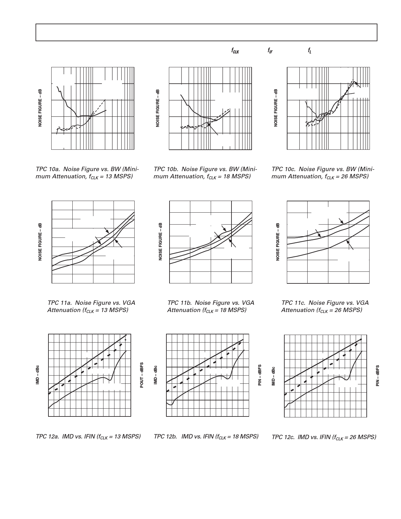
(VDDI = VDDF = VDDA = VDDC = VDDL = VDDD = VDDH = VDDx, VDDQ = VDDP = 5.0 V, fCLK = 18 MSPS, fIF = 109.56 MHz, fLO = 107.4 MHz,
TA = 25؇C, LO = –5 dBm, LO and CLK Synthesizer Disabled, 16-Bit Data with AGC and DVGA enabled, unless otherwise noted.)1
10.0
16-BIT
9.5 I/Q DATA
9.0
16-BIT
I/Q DATA
w/ DVGA
ENABLED
10.0
9.5
16-BIT
DATA
9.0
16-BIT DATA
w/ DVGA
ENABLED
10.0
16-BIT DATA
w/ DVGA
ENABLED
9.5
16-BIT
DATA
9.0
24-BIT
DATA
8.5 8.5 8.5
8.0
24-BIT
I/Q DATA
7.5
10
100
CHANNEL BANDWIDTH – kHz
1000
TPC 10a. Noise Figure vs. BW (Mini-
mum Attenuation, fCLK = 13 MSPS)
8.0
7.5
10
24-BIT
DATA
100
CHANNEL BANDWIDTH – kHz
1000
TPC 10b. Noise Figure vs. BW (Mini-
mum Attenuation, fCLK = 18 MSPS)
8.0
7.5
10
100
CHANNEL BANDWIDTH – kHz
1000
TPC 10c. Noise Figure vs. BW (Mini-
mum Attenuation, fCLK = 26 MSPS)
11.5
11.0
10.5 BW = 27.08kHz
(K = 0, M = 3)
10.0
BW = 12.04kHz
9.5 (K = 0, M = 8)
9.0
BW = 6.78kHz
8.5 (K = 0, M = 15)
8.0
7.5
7.0
0 3 6 9 12
VGA ATTENUATION – dB
TPC 11a. Noise Figure vs. VGA
Attenuation (fCLK = 13 MSPS)
14
13
BW = 75kHz
12 (K = 0, M = 1)
BW = 50kHz
11 (K = 0, M = 2)
10
BW = 15kHz
(K = 0, M = 9)
9
8
7
0 3 6 9 12
VGA ATTENUATION – dB
TPC 11b. Noise Figure vs. VGA
Attenuation (fCLK = 18 MSPS)
14
13
BW = 135.42kHz
(K = 1, M = 1)
12 BW = 90.28kHz
(K = 1, M = 2)
11
10
BW = 27.08kHz
9 (K = 1, M = 9)
8
7
0 3 6 9 12
VGA ATTENUATION – dB
TPC 11c. Noise Figure vs. VGA
Attenuation (fCLK = 26 MSPS)
–30 –5
–40 –10
–50
PIN
–60
–15
–70 –20
LOW BIAS
–80 –25
–90
–100
–110
–120
HIGH BIAS
–30
–35
–40
–130
–45
–45 –42 –39 –36 –33 –30 –27 –24
IFIN – dBm
TPC 12a. IMD vs. IFIN (fCLK = 13 MSPS)
–30 –5
–40 –10
–50
PIN
–60
–15
–70 –20
LOW BIAS
–80 –25
–90
–100
–110
–120
HIGH BIAS
–30
–35
–40
–130
–45
–45 –42 –39 –36 –33 –30 –27 –24
IFIN – dBm
TPC 12b. IMD vs. IFIN (fCLK = 18 MSPS)
–30 –5
–40 –10
–50
PIN
–60
–15
–70 –20
LOW BIAS
–80 –25
–90
–100
–110
–120
HIGH BIAS
–30
–35
–40
–130
–45
–45 –42 –39 –36 –33 –30 –27 –24
IFIN – dBm
TPC 12c. IMD vs. IFIN (fCLK = 26 MSPS)
1Data taken with Toko FSLM series 10 µH inductors.
2High Bias corresponds to LNA_Mixer Setting of 33 in SPI Register 0x01.
3Low Bias corresponds to LNA_Mixer Setting of 12 in SPI Register 0x01.
REV. A
–11–
11 Page | ||
| Páginas | Total 30 Páginas | |
| PDF Descargar | [ Datasheet AD9874.PDF ] | |
Hoja de datos destacado
| Número de pieza | Descripción | Fabricantes |
| AD9870 | IF Digitizing Subsystem | Analog Devices |
| AD9873 | Analog Front End Converter for Set-Top Box/ Cable Modem | Analog Devices |
| AD9874 | IF Digitizing Subsystem | Analog Devices |
| AD9875 | Broadband Modem Mixed-Signal Front End | Analog Devices |
| Número de pieza | Descripción | Fabricantes |
| SLA6805M | High Voltage 3 phase Motor Driver IC. |
Sanken |
| SDC1742 | 12- and 14-Bit Hybrid Synchro / Resolver-to-Digital Converters. |
Analog Devices |
|
DataSheet.es es una pagina web que funciona como un repositorio de manuales o hoja de datos de muchos de los productos más populares, |
| DataSheet.es | 2020 | Privacy Policy | Contacto | Buscar |
