|
|
|
PDF SSM6G18NU Data sheet ( Hoja de datos )
| Número de pieza | SSM6G18NU | |
| Descripción | Silicon Epitaxial Schottky Barrier Diode | |
| Fabricantes | Toshiba Semiconductor | |
| Logotipo | ||
Hay una vista previa y un enlace de descarga de SSM6G18NU (archivo pdf) en la parte inferior de esta página. Total 8 Páginas | ||
|
No Preview Available !
SSM6G18NU
Silicon P Channel MOS Type / Silicon Epitaxial Schottky Barrier Diode
SSM6G18NU
Power Management Switch Applications
• Combined a P-channel MOSFET and a schottky barrier diode in one
package.
• Low RDS (ON) and Low VF
RDS(ON) = 261 m (max) (@VGS = -1.5V)
RDS(ON) = 185 m (max) (@VGS = -1.8 V)
RDS(ON) = 143 m (max) (@VGS = -2.5 V)
RDS(ON) = 112 m (max) (@VGS = -4.5 V)
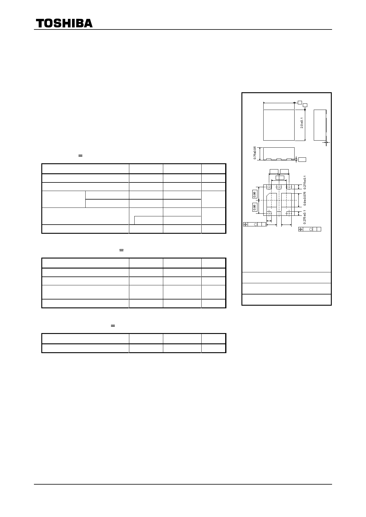
2.0 0.1
Unit: mm
B
A
Absolute Maximum Ratings
MOSFET (Ta = 25°C)
Characteristics
Drain-Source voltage
Gate-Source voltage
Drain current
DC
Pulse
Power dissipation
Channel temperature
Symbol
VDSS
VGSS
ID (Note 1)
IDP (Note 1)
PD(Note 2)
t 10s
Tch
Rating
−20
±8
−2.0
−4.0
1
2
150
Schottky Barrier Diode(Ta = 25°C)
Characteristics
Reverse voltage
Average forward current
Peak one cycle surge forward
current(10ms)
Junction temperature
Symbol
VR
IO
IFSM
Tj
Rating
30
1.0
5.0
150
Unit
V
V
A
W
°C
Unit
V
A
A
°C
MOSFET and Diode (Ta = 25°C)
Characteristics
Storage temperature range
Symbol
Tstg
Rating
−55 to 150
Unit
°C
*BOTTOM VIEW
1
0.65 0.65
0.95
23
0.13
0 0.05
6
0.3 0.075
0.05 M A B
54
0.65 0.075 0.65 0.075
0.05 M A B
1. Anode
2. NC
3. Drain
4. Source
5. Gate
6. Cathode
UDFN6
JEDEC
JEITA
TOSHIBA
2-2Y1A
Weight: 8.5 mg (typ.)
Note:
Note 1:
Note 2:
Using continuously under heavy loads (e.g. the application of high temperature/current/voltage and the
significant change in temperature, etc.) may cause this product to decrease in the reliability significantly
even if the operating conditions (i.e. operating temperature/current/voltage, etc.) are within the absolute
maximum ratings.
Please design the appropriate reliability upon reviewing the Toshiba Semiconductor Reliability Handbook
(“Handling Precautions”/“Derating Concept and Methods”) and individual reliability data (i.e. reliability test
report and estimated failure rate, etc).
The junction temperature should not exceed 150°C during use.
Mounted on FR4 board.
(25.4 mm × 25.4 mm × 1.6 mm, Cu Pad: 645mm2)
1 2010-09-30
1 page 
10
Common Source
VDS = -3 V
Ta = 25°C
Pulse test
3
|Yfs| – ID
1
0.3
0.1
-0.01
-0.1 -1
Drain current ID (A)
-10
1000
C – VDS
300
Ciss
100
30 Common Source
Ta = 25 °C
f = 1 MHz
VGS = 0 V
10
-0.1
-1
Coss
Crss
-10
Drain-source voltage VDS (V)
-100
SSM6G18NU
10
Common Source
VGS = 0 V
Pulse test
D
1
G IDR
IDR – VDS
S
0.1
-25 °C
0.01
Ta =100 °C
25 °C
0.001
0
0.5 1.0
Drain–source voltage VDS (V)
1.5
10000
toff
1000
tf
100
t – ID
Common Source
VDD = -10 V
VGS = 0 to -2.5 V
Ta = 25 °C
RG = 4.7Ω
ton
10
tr
1
-0.001
-0.01
-0.1
-1
Drain current ID (A)
-10
Dynamic Input Characteristic
-8
Common Source
ID = -2.0 A
Ta = 25°C
-6
VDD = - 10 V
-4
VDD = - 16 V
-2
0
02
4 6 8 10
Total Gate Charge Qg (nC)
5
2010-09-30
5 Page | ||
| Páginas | Total 8 Páginas | |
| PDF Descargar | [ Datasheet SSM6G18NU.PDF ] | |
Hoja de datos destacado
| Número de pieza | Descripción | Fabricantes |
| SSM6G18NU | Silicon Epitaxial Schottky Barrier Diode | Toshiba Semiconductor |
| Número de pieza | Descripción | Fabricantes |
| SLA6805M | High Voltage 3 phase Motor Driver IC. |
Sanken |
| SDC1742 | 12- and 14-Bit Hybrid Synchro / Resolver-to-Digital Converters. |
Analog Devices |
|
DataSheet.es es una pagina web que funciona como un repositorio de manuales o hoja de datos de muchos de los productos más populares, |
| DataSheet.es | 2020 | Privacy Policy | Contacto | Buscar |