|
|
|
PDF HC-5504B1 Data sheet ( Hoja de datos )
| Número de pieza | HC-5504B1 | |
| Descripción | ITU Low Cost/ PABX SLIC With 40mA Loop Feed | |
| Fabricantes | Intersil Corporation | |
| Logotipo | ||
Hay una vista previa y un enlace de descarga de HC-5504B1 (archivo pdf) en la parte inferior de esta página. Total 9 Páginas | ||
|
No Preview Available !
Data Sheet
HC-5504B1
February 1999 File Number 4125.3
ITU Low Cost, PABX SLIC With 40mA
Loop Feed
The Intersil SLIC incorporates many of the BORSHT
functions on a single IC chip. This includes DC battery feed,
a ring relay driver, supervisory and hybrid functions. This
device is designed to maintain transmission performance in
the presence of externally induced longitudinal currents.
Using the unique Intersil dielectric isolation process, the
SLIC can operate directly with a wide range of station
battery voltages.
The SLIC also provides selective denial of power. If the PBX
system becomes overloaded during an emergency, the SLIC
will provide system protection by denying power to selected
subscriber loops.
The Intersil SLIC is ideally suited for the design of new digital
PBX systems by eliminating bulky hybrid transformers.
Ordering Information
TEMP.
PART NUMBER RANGE (oC) PACKAGE
HC4P5504B1-5
0 to 75 28 Ld PLCC
PKG. NO.
N28.45
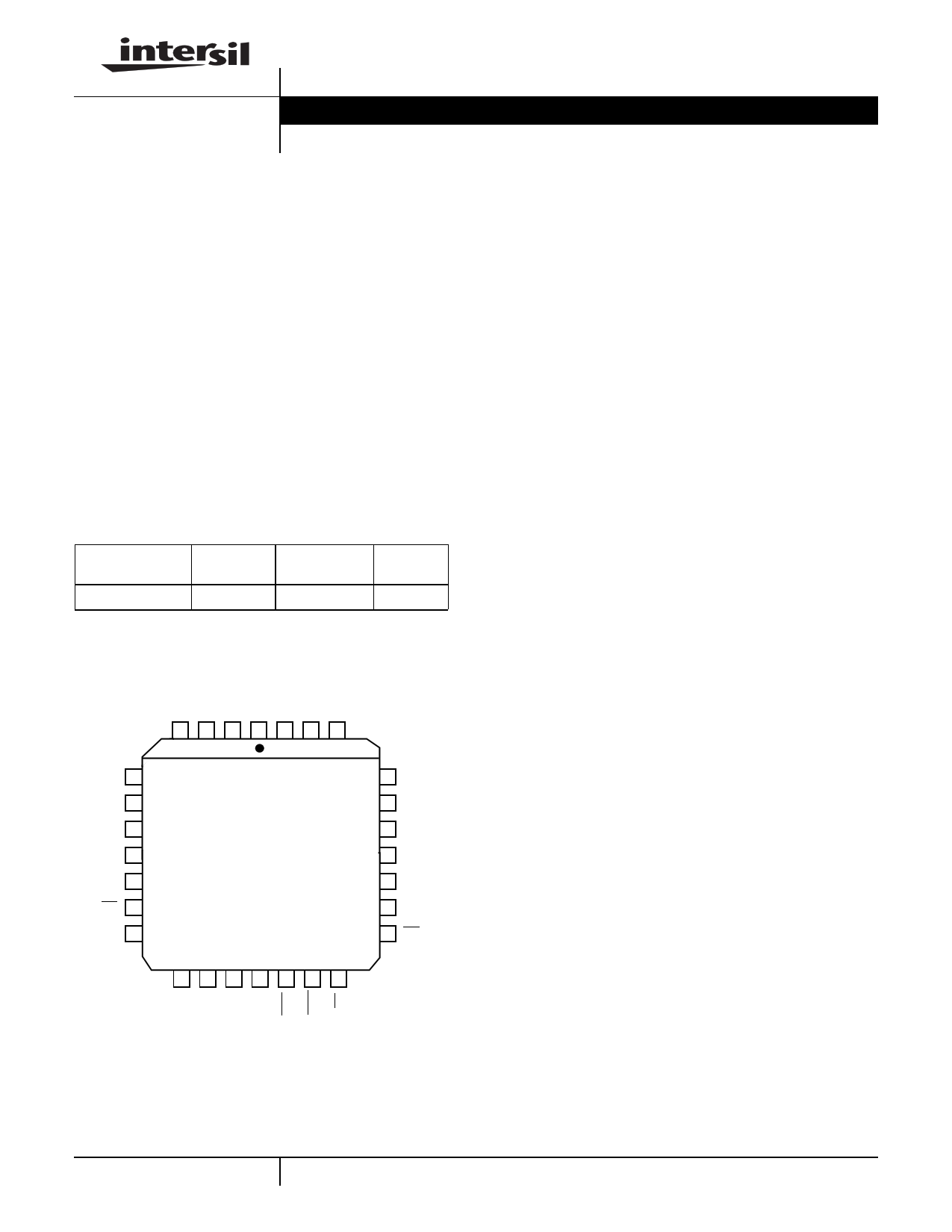
Pinout
HC-5504B1 (PLCC)
TOP VIEW
4 3 2 1 28 27 26
VB+ 5
C3 6
DG 7
N/C 8
RS 9
RD 10
TF 11
25 RX
24 +IN
23 -IN
22 N/C
21 OUT
20 C2
19 RC
12 13 14 15 16 17 18
Features
• Low Cost Version of the HC-5504B
• Capable of 5V or 12V (VB+) Operation
• Monolithic Integrated Device
• DI High Voltage Process
• Compatible With Worldwide PBX Performance
Requirements
• Controlled Supply of Battery Feed Current for Short Loops
(41mA)
• Internal Ring Relay Driver
• Allows Interfacing With Negative Superimposed Ringing
Systems
• Low Power Consumption During Standby
• Switch Hook Ground Key and Ring Trip Detection
Functions
• Selective Denial of Power to Subscriber Loops
Applications
• Solid State Line Interface Circuit for Analog and Digital
PBX Systems
• Direct Inward Dial (DID) Trunks
• Voice Messaging PBXs
• Related Literature
- AN549, The HC-5502S/4X Telephone Subscriber Line
Interface Circuits (SLIC)
- AN571, Using Ring Sync with HC-5502A and HC-5504
SLICs
52 CAUTION: These devices are sensitive to electrostatic discharge; follow proper IC Handling Procedures.
http://www.intersil.com or 407-727-9207 | Copyright © Intersil Corporation 1999
1 page 
HC-5504B1
Pin Descriptions
28 PIN
PLCC
2
3
4
5
6
7
9
10
11
12
13
14
16
17
18
19
20
21
23
24
25
SYMBOL
DESCRIPTION
TIP An analog input connected to the TIP (more positive) side of the subscriber loop through a 150Ω feed resistor and a ring
relay contact. Functions with the Ring terminal to receive voice signals from the telephone and for loop monitoring pur-
poses.
RING
An analog input connected to the RING (more negative) side of the subscriber loop through a 150Ω feed resistor and a
ring relay contact. Functions with the Tip terminal to receive voice signals from the telephone and for loop monitoring pur-
poses.
RFS
Senses ring side of loop for ground key and ring trip detection. During ringing, the ring signal is inserted into the line at
this node and RF is isolated from RFS via a relay.
VB+ Positive Voltage Source - Most positive supply. VB+ is typically 12V or 5V.
C3 Capacitor #3 - An external capacitor to be connected between this terminal and analog ground. Required for proper op-
eration of the loop current limiting function, and for filtering VB-. Typical value is 0.3µF, 30V.
DG Digital Ground - To be connected to zero potential and serves as a reference for all digital inputs and outputs on the SLIC
microcircuit.
RS Ring Synchronization Input - A TTL - compatible clock input. The clock should be arranged such that a positive pulse
transition occurs on the zero crossing of the ring voltage source, as it appears at the RFS terminal. For Tip side injected
systems, the RS pulse should occur on the negative going zero crossing and for Ring injected systems, on the positive
going zero crossing. This ensures that the ring relay activates and deactivates when the instantaneous ring voltage is
near zero. If synchronization is not required, the pin should be tied to 5V.
RD Relay Driver - A low active open collector logic output. When enabled, the external ring relay is energized.
TF Tip Feed - A low impedance analog output connected to the TIP terminal through a 150Ω feed resistor. Functions with
the RF terminal to provide loop current, feed voice signals to the telephone set, and sink longitudinal current.
RF Ring Feed - A low impedance analog output connected to the RING terminal through a 150Ω feed resistor. Functions with
the TF terminal to provide loop current, feed voice signals to the telephone set, and sink longitudinal current.
VB- Negative Voltage Source - Most negative supply. VB- is typically -48V with an operational range of -42V to -58V. Frequent-
ly referred to as “battery”.
BG Battery Ground - To be connected to zero potential. All loop current and some quiescent current flows into this ground
terminal.
SHD
Switch Hook Detection - A low active LS TTL-compatible logic output. This output is enabled for loop currents exceeding
10mA and disabled for loop currents less than 5mA.
GKD
Ground Key Detection - A low active LS TTL-compatible logic output. This output is enabled if the DC current into the ring
lead exceeds the DC current out of the tip lead by more than 20mA, and disabled if this current difference is less than
10mA.
PD Power Denial - A low active TTL - Compatible logic input. When enabled, the switch hook detect (SHD) and ground key
detect (GKD) are not necessarily valid, and the relay driver (RD) output is disabled.
RC Ring Command - A low active TTL - Compatible logic input. When enabled, the relay driver (RD) output goes low on the
next high level of the ring sync (RS) input, as long as the SLIC is not in the power denial state (PD = 0) or the subscriber
is not already off- hook (SHD = 0).
C2 Capacitor #2 - An external capacitor to be connected between this terminal and digital ground. Prevents false ground key
indications from occurring during ring trip detection. Typical value is 0.15µF, 10V. This capacitor is not used if ground key
function is not required and (Pin 17) may be left open or connected to digital ground.
OUT The analog output of the spare operational amplifier. The output voltage swing is typically ±5V.
-IN The inverting analog input of the spare operational amplifier.
+IN The non-inverting analog input of the spare operational amplifier.
RX Receive Input, Four Wire Side - A high impedance analog input which is internally biased. Capacitive coupling to this input
is required. AC signals appearing at this input differentially drive the Tip feed and Ring feed terminals, which in turn drive
tip and ring through 300Ω of feed resistance on each side of the line.
56
5 Page | ||
| Páginas | Total 9 Páginas | |
| PDF Descargar | [ Datasheet HC-5504B1.PDF ] | |
Hoja de datos destacado
| Número de pieza | Descripción | Fabricantes |
| HC-5504B | EIA/ITU PABX SLIC with 40mA Loop Feed | Intersil Corporation |
| HC-5504B1 | ITU Low Cost/ PABX SLIC With 40mA Loop Feed | Intersil Corporation |
| Número de pieza | Descripción | Fabricantes |
| SLA6805M | High Voltage 3 phase Motor Driver IC. |
Sanken |
| SDC1742 | 12- and 14-Bit Hybrid Synchro / Resolver-to-Digital Converters. |
Analog Devices |
|
DataSheet.es es una pagina web que funciona como un repositorio de manuales o hoja de datos de muchos de los productos más populares, |
| DataSheet.es | 2020 | Privacy Policy | Contacto | Buscar |