|
|
|
PDF NOIV1SN025KA-GWC Data sheet ( Hoja de datos )
| Número de pieza | NOIV1SN025KA-GWC | |
| Descripción | VITA 25K Image Sensor | |
| Fabricantes | ON Semiconductor | |
| Logotipo | ||
Hay una vista previa y un enlace de descarga de NOIV1SN025KA-GWC (archivo pdf) en la parte inferior de esta página. Total 30 Páginas | ||
|
No Preview Available !
NOIV1SN025KA
VITA 25K Image Sensor
Features
• 5120 x 5120 Active Pixels
• 4.5 mm x 4.5 mm Square Pixels
• 35 mm Optical Format
• Monochrome (SN) or Color (SE)
• 53 Frames per Second (fps) at Full Resolution
• On-chip 10-bit Analog-to-Digital Converter (ADC)
• 32 Low-voltage Differential Signaling (LVDS) High-speed Serial
Outputs
• Random Programmable Region of Interest (ROI) Readout
• Pipelined and Triggered Global Shutter, Rolling Shutter
• On-chip Fixed Pattern Noise (FPN) Correction
• Serial Peripheral Interface (SPI)
• Operational Range: −40°C to +85°C
• 355-pin mPGA Package
• 3.4 W Power Dissipation
• These Devices are Pb−Free and are RoHS Compliant
http://onsemi.com
Applications
• Machine Vision
• Motion Monitoring
• Intelligent Traffic Systems (ITS)
• Pick and Place Machines
• Inspection
• Metrology
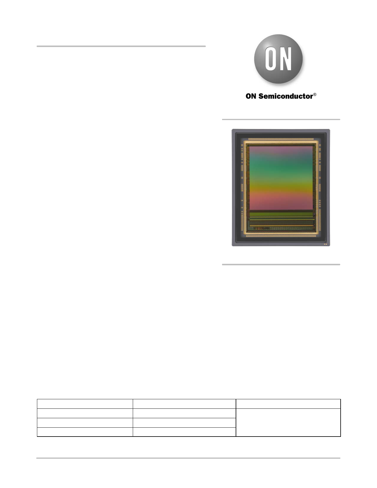
Figure 1. VITA 25K Photograph
Description
The VITA 25K is a 5120 x 5120 CMOS image sensor delivering high resolution images at frame rates up to 53 frames per
second. The high sensitivity 4.5 mm x 4.5 mm pixels support pipelined and triggered global shutter readout modes and can also
be operated in a low noise rolling shutter mode. In rolling shutter mode, the sensor supports correlated double sampling readout,
reducing noise and increasing the dynamic range.
The sensor has on-chip programmable gain amplifiers and 10-bit A/D converters. The image’s black level is either calibrated
automatically or can be adjusted by adding a user programmable offset.
A high level of programmability using a four wire serial peripheral interface enables the user to read out specific regions
of interest. Up to 32 regions can be programmed, achieving even higher frame rates.
The image data interface consists of 32 LVDS lanes. Each channel runs at 620 Mbps. A separate synchronization channel
containing payload information is provided to facilitate the image reconstruction at the receive end.
The VITA 25K is packaged in a ceramic 355-pin mPGA package and is available in a monochrome, color and windowless
versions.
Contact your local ON Semiconductor office for more information.
ORDERING INFORMATION
Part Number
NOIV1SN025KA-GDC
NOIV1SE025KA-GDC
NOIV1SN025KA-GWC
Description
Mono micro lens
Color micro lens
Mono micro lens windowless
Package
355−mPGA
© Semiconductor Components Industries, LLC, 2014
June, 2014 − Rev. 9
1
Publication Order Number:
NOIV1SN025KA/D
1 page 
NOIV1SN025KA
Electrical Specifications
Power Supply Ratings
Table 5. POWER SUPPLY RATINGS
Limits in bold apply for for TJ = TMIN to TMAX, all other limits TJ = +30°C [5], [6], [7], [8]
Parameter
Description
Power Supply Parameters
vdda_33
Analog supply - 3.3 V domain. gnda_33 is connected to substrate
Idda_33
Current consumption from analog supply
vddd_33
Digital supply - 3.3 V domain. gndd_33 is connected to substrate
Iddd_33
Current consumption from 3.3 V digital supply
vdd_18
Digital supply - 1.8 V domain. gndd_18 is connected to substrate
Idd_18
Current consumption 1.8 V digital supply
vdd_pix
Pixel array supply
Idd_pix
Current consumption from pixel supply
vdd_resfd
Floating diffusion reset supply
gnd_resfd
Floating diffusion reset ground. Not connected to substrate
vdd_respd
Photo diode reset supply
gnd_respd
Photo diode reset ground. Not connected to substrate.
Note This is a sinking power supply with 200 mA range.
Min
3
675
3
65
1.6
240
3
25
3.3
0
3.3
0
Typ
3.3
725
3.3
85
1.8
310
3.3
35
4.5
0
4.2
0
vdd_trans
Pixel transfer supply
3.3 4.2
gnd_trans
Pixel transfer ground. Not connected to substrate
00
vdd_sel
Pixel select supply
3.0 3.3
gnd_sel
Pixel select ground. Not connected to substrate.
00
vdd_casc
Cascode supply
vref_colmux [8] Column multiplexer reference supply
0.9 1.0
– 1.0
gnd_colbias
Column biasing ground. Dedicated ground signal for pixel biasing.
Connected to substrate
–
0
gnd_colpc
Column precharge ground. Dedicated ground signal for pixel bias-
ing. Not connected to substrate
–
0
Ptot Total power consumption
3000
3400
Pstby
Power consumption in standby mode
––
Popt
Power consumption at lower pixel rates
Configurable
I/O - LVDS (EIA/TIA-644): Conforming to standard/additional specifications and deviations listed
fserdata
Data rate on data channels in 10-bit mode
DDR signaling - 32 data channels, 1 synchronization channel
fserdata
Data rate on data channels in 8-bit mode
DDR signaling - 32 data channels, 1 synchronization channel
fserclock
Clock rate of output clock in 10-bit mode
Clock output for mesochronous signaling
fserclock
Clock rate of output clock in 8-bit mode
Clock output for mesochronous signaling
Vicm
LVDS input common mode level
0.3 1.25
Tccsk
Channel to channel skew (training pattern allows per-channel skew
correction)
LVDS Electrical/Interface
fin Input clock rate for 10-bit mode
fin Input clock rate for 8-bit mode
Max
3.6
775
3.6
105
2
380
3.6
45
4.6
1.0
4.6
1.0
4.6
1.0
3.6
0
1.1
–
–
–
3800
50
620
496
310
248
2.2
50
310
248
http://onsemi.com
5
Units
V
mA
V
mA
V
mA
V
mA
V
V
V
V
V
V
V
V
V
V
V
V
mW
mW
Mbps
Mbps
MHz
MHz
V
ps
MHz
MHz
5 Page 
NOIV1SN025KA
OPERATING MODES
This sensor supports multiple operation modes. The
following list provides an overview.
• Global Shutter mode
♦ Pipelined global shutter mode
- Master mode
- Slave mode
♦ Triggered global shutter
- Master mode
- Slave mode
• Rolling shutter mode
• Multiple windowing readout
♦ Flexible window configuration
♦ Processing multiple windows in Global Shutter
mode
• Subsampling and binning
♦ Pixel binning
♦ Subsampling
a frame overhead time (FOT), during which the analog value
on the pixel diode is transferred to the pixel memory
element. After the FOT, the sensor is read out line by line and
the readout of each line is preceded by the row overhead time
(ROT).
Global Shutter Mode
In a global shutter mode, light integration takes place on
all pixels in sync, although subsequent readout is sequential,
as shown in Figure 7. Figure 8 shows the integration and
readout sequence for the global shutter. All pixels are light
sensitive at the same time. The whole pixel core is reset
simultaneously and, after the integration time, all pixel
values are sampled together on the storage node inside each
pixel. The pixel core is read out line by line after integration.
The integration and readout can occur in parallel or
sequentially.
The integration starts at a certain period, relative to the
frame start.
Pipelined Global Shutter Mode
In pipelined shutter mode, the integration and readout are
done in parallel. Images are continuously read and
integration of frame N is ongoing during readout of the
previous frame N–1. The readout of every frame starts with
Figure 7. Global Shutter Operation
Master Mode
In this operation mode, the integration time is set through
the register interface and the sensor integrates and reads out
the images autonomously. The sensor acquires images
without any user interaction.
Slave Mode
The slave mode adds more manual control to the sensor.
The integration time registers are ignored in this mode and
the integration time is instead controlled by an external pin.
As soon as the control pin is asserted, the pixel array goes out
of reset and integration starts. The integration continues
until the user or system deasserts the external pin. Upon a
falling edge of the trigger input, the image is sampled and the
readout begins.
Integration Tim e
Handling
Reset
N
Exposure Time N
FOT
Reset
N+1
Exposure Time N+1
FOT
Readout
Handling
FOT
Readout Fram e N -1
FOT
R eadout Fram e N
FOT
ÉÉÉÉÉÉÉÉÉÉÉÉÉÉÉÉÉÉÉÉÉÉÉÉÉÉÉÉÉÉÉÉÉÉÉÉ
ROT
Line Readout
Figure 8. Integration and Readout for Pipelined Shutter
http://onsemi.com
11
11 Page | ||
| Páginas | Total 30 Páginas | |
| PDF Descargar | [ Datasheet NOIV1SN025KA-GWC.PDF ] | |
Hoja de datos destacado
| Número de pieza | Descripción | Fabricantes |
| NOIV1SN025KA-GWC | VITA 25K Image Sensor | ON Semiconductor |
| Número de pieza | Descripción | Fabricantes |
| SLA6805M | High Voltage 3 phase Motor Driver IC. |
Sanken |
| SDC1742 | 12- and 14-Bit Hybrid Synchro / Resolver-to-Digital Converters. |
Analog Devices |
|
DataSheet.es es una pagina web que funciona como un repositorio de manuales o hoja de datos de muchos de los productos más populares, |
| DataSheet.es | 2020 | Privacy Policy | Contacto | Buscar |