|
|
|
PDF SKY77518 Data sheet ( Hoja de datos )
| Número de pieza | SKY77518 | |
| Descripción | TX-RX iPAC FEM | |
| Fabricantes | Skyworks | |
| Logotipo | ||
Hay una vista previa y un enlace de descarga de SKY77518 (archivo pdf) en la parte inferior de esta página. Total 14 Páginas | ||
|
No Preview Available !
PRELIMINARY DATA SHEET
SKY77518 TX–RX iPAC™ FEM for Dual-Band GSM/GPRS
Applications
• Dual-band cellular handsets
encompassing
- Class 4 GSM900
- DCS1800
- Class 12 GPRS multi-slot
operation
Features
• High efficiency
- DCS 41%
- GSM900 46%
• Low transmit supply current
- GSM900 1.3 A
- DCS1800 0.9 A
• Internal ICC sense resistor for iPAC
• Closed loop iPAC
• 50 Ω matched Input/Output
• TX–VCO-to-antenna and antenna-
to-Rx-SAW filter RF interface
• TX harmonics below –33 dBm
• PHEMT RF switches afford high
linearity, low insertion loss, and
less than 20 µA supply current in
receive modes
• Small outline: 6 mm x 8 mm
• Low profile: 1.2 mm
• Compatible with multiple logic
families
• Low APC current: 25 µA
• Gold plated, lead free contacts
Skyworks offers lead
(Pb)-free "environmentally
friendly" packaging
that is RoHS compliant
(European Parliament
for the Restriction of
Hazardous Substances).
Description
The SKY77518 is a transmit and receive front-end module (FEM) with Integrated Power
Amplifier Control (iPAC™) for dual-band cellular handsets comprising GSM900 and DCS1800
operation. Designed in a low profile, compact form factor, the SKY77518 offers a complete
Transmit VCO-to-Antenna and Antenna-to-Receive SAW filter solution. The FEM also supports
Class 12 General Packet Radio Service (GPRS) multi-slot operation.
The module consists of a GSM900 PA block and a DCS1800 PA block, impedance-matching
circuitry for 50 Ω input and output impedances, TX harmonics filtering, high linearity and low
insertion loss PHEMT RF switches, diplexer and a Power Amplifier Control (PAC) block with
internal current sense resistor. A custom BiCMOS integrated circuit provides the internal PAC
function and decoder circuitry to control the RF switches. The two Heterojunction Bipolar
Transistor (HBT) PA blocks are fabricated onto a single Gallium Arsenide (GaAs) die. One PA
block supports the GSM900 band and the other PA block supports the DCS1800 band. Both PA
blocks share common power supply pads to distribute current. The output of each PA block
and the outputs to the two receive pads are connected to the antenna pad through PHEMT RF
switches and a diplexer. The GaAs die, PHEMT die, Silicon (Si) die and passive components are
mounted on a multi-layer laminate substrate. The assembly is encapsulated with plastic
overmold.
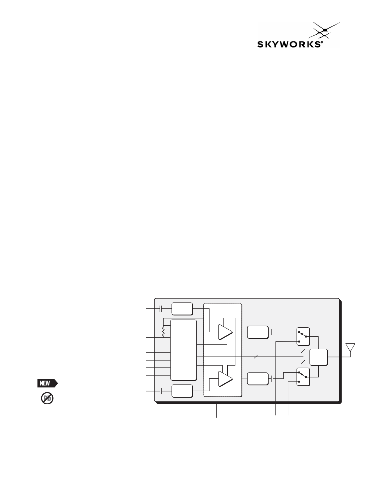
Band selection and control of transmit and receive modes are performed using two external
control pads. Refer to the functional block diagram in Figure 1 below. The band select pad (BS)
selects between GSM and DCS modes of operation. The transmit enable (TX_EN) pad controls
receive or transmit mode of the respective RF switch (TX = logic 1). Proper timing between
transmit enable (TX_EN) and Analog Power Control (VRAMP) allows for high isolation between
the antenna and TX-VCO while the VCO is being tuned prior to the transmit burst.
The SKY77518 is compatible with logic levels from 1.2 V to VCC for BS and TX_EN pads,
depending on the level applied to the VLOGIC pad. This feature provides additional flexibility for
the designer in the selection of FEM interface control logic.
GSM_IN
VBATT
VRAMP
TX_EN
BS
VLOGIC
DCS
Match
BiCMOS
Integrated
Power
Amplifier
Controller
Antenna
Switch
Decoder
Match
HBT
GSM_OUT
PA Match/
Filter
4
DCS_OUT
PA
Match/
Filter
SKY77518
2
Diplexer
2
GND GSM_RX
Figure 1. Functional Block Diagram
DCS_RX
200472_001
Skyworks Solutions, Inc. • Phone [781] 376-3000 • Fax [781] 376-3100 • [email protected] • www.skyworksinc.com
200472P1 • Skyworks Proprietary and Confidential Information • Products and Product Information are Subject to Change Without Notice. • November 9, 2005
1
1 page 
SKY77518 TX–Rx IPAC™ FEM FOR DUAL-BAND GSM/GPRS
PRELIMINARY DATA SHEET
Table 4. SKY77518 Electrical Specifications 1 (3 of 5)
GSM900 Mode (f = 880 to 915 MHz and PIN = 0 to 6 dBm) [continued]
Parameter
Symbol
Test Condition
Minimum Typical Maximum
Units
Spurious
Load mismatch
Spur
Load
Rx Band Spurious
Rx_SPUR
Power control dynamic range
PCDR
Power control
variation
Control level 5-15
(VCC ≥ 3.3 V)
PCV
Control level 16-19
Power control slope
PCS
All combinations of the following
parameters:
VRAMP = controlled 2
PIN = min. to max.
VCC = 2.7 V to 5.5 V
Load VSWR = 12:1, all phase angles
All combinations of the following
parameters:
VRAMP = controlled 2
PIN = min. to max.
VCC = 2.7 V to 5.5 V
Load VSWR = 20:1, all phase angles
At f0 + 20 MHz (935 to 960 MHz)
RBW = 100 kHz
VCC = 3.3 V
5 dBm ≤ POUT ≤ 33 dBm
TCASE = +25 °C
At f0 + 10 MHz (925 to 935 MHz)
RBW = 100 kHz
VCC = 3.3 V
TCASE = +25 °C
5 dBm ≤ POUT ≤ 33 dBm
At 1805 to 1880 MHz
RBW = 100 kHz
VCC = 3.3 V
TCASE = +25 °C
5 dBm ≤ POUT ≤ 33 dBm
POUT 13 to 33 dBm, +25 °C
POUT 13 to 33 dBm
POUT 5 to 11 dBm, +25 °C
POUT 5 to 11 dBm
5 to 33 dBm
No parasitic oscillation > –36 dBm
No module damage or permanent degradation
⎯ — –82
⎯ –80 –76 dBm
⎯ –101 –84
30 50 ⎯ dB
–1.0 ⎯ +1.0
–2.0 ⎯ +2.0 dB
–2.0 ⎯ +2.0
–3.5 ⎯ +3.5
⎯ ⎯ 150 dB/V
GSM900 RECEIVE (f = 925 to 960 MHz) Mode = GSM_Rx
Parameter
Frequency range
Insertion Loss, ANT to GSM_Rx 4
VSWR ANT, GSM_Rx 4
Symbol
f
IL GSM_Rx
ΓIN, ΓOUT
Test Condition
—
—
—
Minimum
925
⎯
⎯
Typical
⎯
1.0
1.2:1
Maximum
960
1.3
1.5:1
Units
MHz
dB
Skyworks Solutions, Inc. • Phone [781] 376-3000 • Fax [781] 376-3100 • [email protected] • www.skyworksinc.com
200472P1 • Skyworks Proprietary and Confidential Information • Products and Product Information are Subject to Change Without Notice. • November 9, 2005
5
5 Page 
SKY77518 TX–Rx IPAC™ FEM FOR DUAL-BAND GSM/GPRS
PRELIMINARY DATA SHEET
1 TYP
0.5
0.85
8
4X 1.88
Component
6
Outline
STENCIL APERTURE
TOP VIEW
(0%-20% reduction of openings
for Center Ground Pads by area.
Shown same as package footprint.)
1 TYP
A
8.6 8
4
6
6.6
SOLDER MASK OPENING
TOP VIEW
Component
Outline
1 TYP
2X 1.1
8.5 8
A
Common
Ground
Pads
0.25 TYP
6
6.5
METALLIZATION
TOP VIEW
(1.1)
(2)
PAD
SOLDER MASK
Thermal Via Array (4 rows x 5 columns)
Ø0.3 mm on 0.6 mm Pitch
Additional vias in Common Ground Pad
will improve thermal performance.
NOTE: Thermal vias should be
tented and filled with solder mask,
30-35 µm copper plating recommended.
0.95
0.85
0.5 0.6
DETAIL A
20X
Component
Outline
ALL DIMENSIONS IN MILLIMETERS.
200472_006
Figure 6. Phone PCB Layout Footprint for 6 x 8 mm, 20-Pad Package with Grid-Bottom Solder Mask – SKY77518 Specific.
Skyworks Solutions, Inc. • Phone [781] 376-3000 • Fax [781] 376-3100 • [email protected] • www.skyworksinc.com
200472P1 • Skyworks Proprietary and Confidential Information • Products and Product Information are Subject to Change Without Notice. • November 9, 2005
11
11 Page | ||
| Páginas | Total 14 Páginas | |
| PDF Descargar | [ Datasheet SKY77518.PDF ] | |
Hoja de datos destacado
| Número de pieza | Descripción | Fabricantes |
| SKY77517-21 | TX-RX iPAC FEM | Skyworks Solutions |
| SKY77518 | TX-RX iPAC FEM | Skyworks |
| SKY77518-21 | FEM FOR DUAL-BAND GSM/GPRS | Skyworks |
| SKY77519 | TX-RX FEM | Skyworks Solutions |
| Número de pieza | Descripción | Fabricantes |
| SLA6805M | High Voltage 3 phase Motor Driver IC. |
Sanken |
| SDC1742 | 12- and 14-Bit Hybrid Synchro / Resolver-to-Digital Converters. |
Analog Devices |
|
DataSheet.es es una pagina web que funciona como un repositorio de manuales o hoja de datos de muchos de los productos más populares, |
| DataSheet.es | 2020 | Privacy Policy | Contacto | Buscar |