|
|
|
PDF AUR9717 Data sheet ( Hoja de datos )
| Número de pieza | AUR9717 | |
| Descripción | 1.5MHz PWM Step-down DC-DC Converter | |
| Fabricantes | BCD | |
| Logotipo | ||
Hay una vista previa y un enlace de descarga de AUR9717 (archivo pdf) en la parte inferior de esta página. Total 14 Páginas | ||
|
No Preview Available !
Data Sheet
Dual 1A, 1.5MHz PWM Step-down DC-DC Converter with OVP
AUR9717
General Description
The AUR9717 is a high efficiency step-down
DC-DC voltage converter. The chip operation is
optimized using constant frequency, peak-current
mode architecture with built-in synchronous power
MOSFET switchers and internal compensators to
reduce external part counts. It is automatically
switching between the normal PWM mode and LDO
mode to offer improved system power efficiency
covering a wide range of loading conditions.
The oscillator and timing capacitors are all built-in
providing an internal switching frequency of 1.5MHz
that allows the use of small surface mount inductors
and capacitors for portable product implementations.
Additional features including Soft Start (SS), Under
Voltage Lock Out (UVLO), Input Over Voltage
Protection (IOVP) and Thermal Shutdown Detection
(TSD) are integrated to provide reliable product
applications.
The device is available in adjustable output voltage
versions ranging from 1V to 3.3V, and is able to
deliver up to 1A.
The AUR9717 is available in WDFN-3×3-10
package.
Features
• Dual Channel High Efficiency Buck Power
Converter
• Low Quiescent Current
• Output Current: 1A
• Adjustable Output Voltage from 1V to 3.3V
• Wide Operating Voltage Range: 2.5V to 5.5V
• Built-in Power Switchers for Synchronous
Rectification with High Efficiency
• Feedback Voltage: 600mV
• 1.5MHz Constant Frequency Operation
• Automatic PWM/LDO Mode Switching Control
• Thermal Shutdown Protection
• Low Drop-out Operation at 100% Duty Cycle
• No Schottky Diode Required
• Internal Input Over Voltage Protection
Applications
• Mobile Phone, Digital Camera and MP3 Player
• Headset, Radio and Other Hand-held Instruments
• Post DC-DC Voltage Regulation
• PDA and Notebook Computer
Oct. 2011 Rev. 1.0
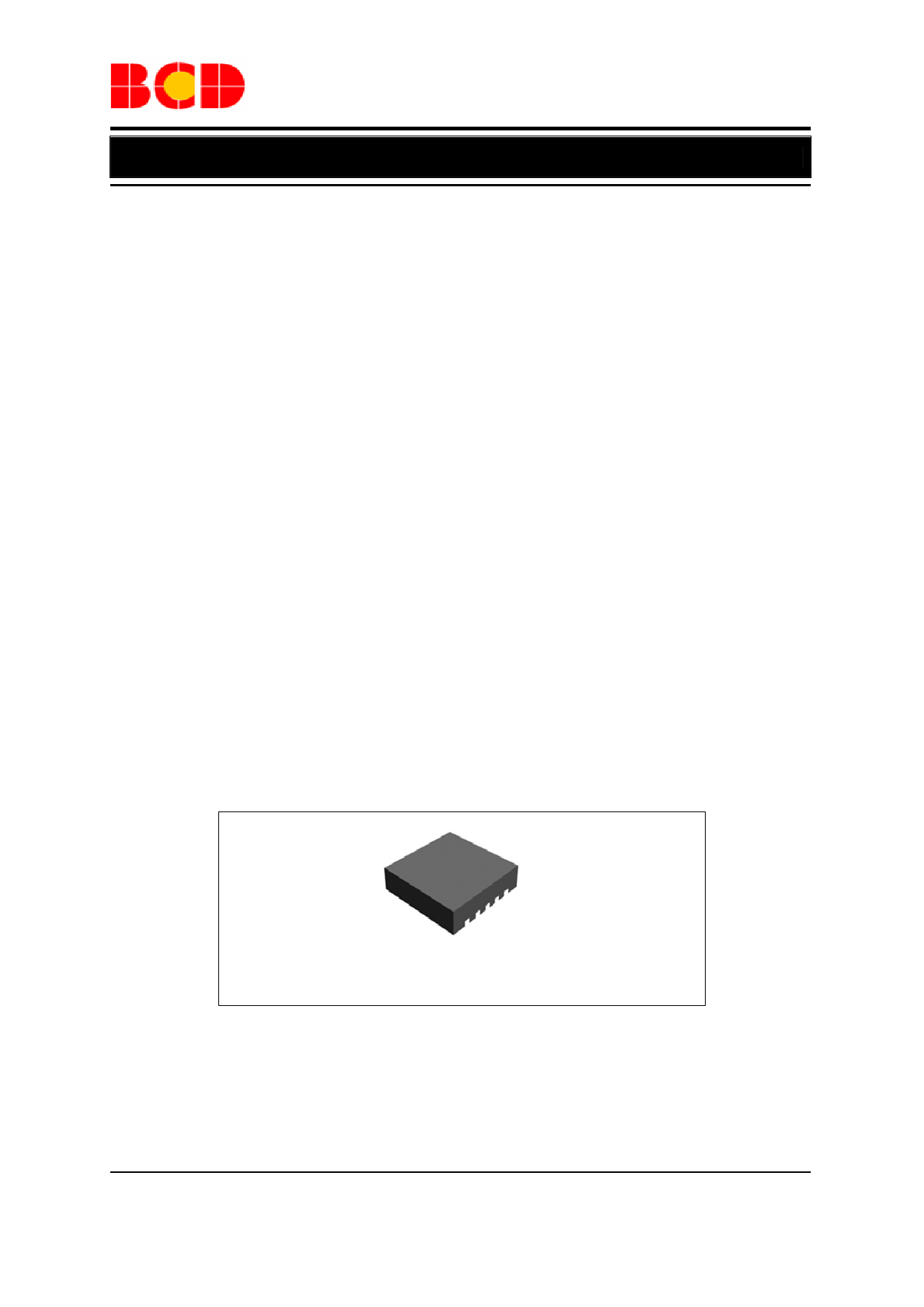
WDFN-3×3-10
Figure 1. Package Type of AUR9717
BCD Semiconductor Manufacturing Limited
1
1 page 
Data Sheet
Dual 1A, 1.5MHz PWM Step-down DC-DC Converter with OVP
AUR9717
Electrical Characteristics
VIN=VEN1=VEN2=5V, VFB1=VFB2=0.6V, L1=L2=2.2μH, CIN1=CIN2=4.7μF, COUT1=COUT2=10μF, TA=25°C,
unless otherwise specified.
Parameter
Symbol
Input Voltage Range
VIN
Shutdown Current
Regulated Feedback
Voltage
Regulated Output
Voltage Accuracy
Peak
Current
Inductor
IOFF
VFB
ΔVOUT1/VOUT1,
ΔVOUT2/VOUT2
IPK
Oscillator Frequency
PMOSFET RON
NMOSFET RON
fOSC
RON(P)
RON(N)
LX Leakage Current
ILX
Feedback Current
Input Over Voltage
Protection
EN Leakage Current
EN High-level Input
Voltage
EN Low-level Input
Voltage
Under Voltage Lock
Out
Hysteresis
Thermal Shutdown
IFB1, IFB2
VIOVP
IEN1, IEN2
VEN_H1, VEN_H2
VEN_L1, VEN_L2
VUVLO
TSD
Conditions
VIN=VIN1=VIN2
VEN1=VEN2=0V
For Adjustable Output Voltage
VIN=2.5V to 5.5V,
IOUT1=IOUT2=0 to 1A
VFB1=VFB2=0.5V
IOUT1=IOUT2=200mA
IOUT1=IOUT2=200mA
VEN1=VEN2=0V,
VLX1=VLX2=0V or 5V
VIN=2.5V to 5.5V
VIN=2.5V to 5.5V
Rising
Hysteresis
Min Typ Max Unit
2.5 5.5 V
0.1 1 μA
0.585 0.6 0.615 V
-3 3 %
1.5 A
1.2 1.5 1.8 MHz
0.28 Ω
0.25 Ω
0.01 0.1 μA
30 nA
6V
0.01 0.1
1.5
μA
V
0.6 V
1.8 V
0.1 V
160 °C
Oct. 2011 Rev. 1.0
BCD Semiconductor Manufacturing Limited
5
5 Page 
Data Sheet
Dual 1A, 1.5MHz PWM Step-down DC-DC Converter with OVP
AUR9717
Application Information (Continued)
5. Efficiency Considerations
The efficiency of switching regulator is equal to the
output power divided by the input power times 100%.
It is usually useful to analyze the individual losses to
determine what is limiting efficiency and which
change could produce the largest improvement.
Efficiency can be expressed as:
Efficiency=100%-L1-L2-…..
NMOSFET RDS(ON)N resistance and the duty cycle
(D):
( )RSW = RDS (ON )P × D + RDS (ON )N × 1 − D
Therefore, to obtain the I2R losses, simply add RSW to
RL and multiply the result by the square of the
average output current.
Where L1, L2, etc. are the individual losses as a
percentage of input power.
Although all dissipative elements in the regulator
produce losses, two major sources usually account for
most of the power losses: VIN quiescent current and
I2R losses. The VIN quiescent current loss dominates
the efficiency loss at very light load currents and the
I2R loss dominates the efficiency loss at medium to
heavy load currents.
5.1 The VIN quiescent current loss comprises two
parts: the DC bias current as given in the electrical
characteristics and the internal MOSFET switch gate
charge currents. The gate charge current results from
switching the gate capacitance of the internal power
MOSFET switches. Each cycle the gate is switched
from high to low, then to high again, and the packet
of charge, dQ moves from VIN to ground. The
resulting dQ/dt is the current out of VIN that is
typically larger than the internal DC bias current. In
continuous mode,
I GATE = f × (QP + QN )
Where QP and QN are the gate charge of power
PMOSFET and NMOSFET switches. Both the DC
bias current and gate charge losses are proportional to
the VIN and this effect will be more serious at higher
input voltages.
Other losses including CIN and COUT ESR dissipative
losses and inductor core losses generally account for
less than 2% of total additional loss.
6. Thermal Characteristics
In most applications, the part does not dissipate much
heat due to its high efficiency. However, in some
conditions when the part is operating in high ambient
temperature with high RDS(ON) resistance and high
duty cycles, such as in LDO mode, the heat
dissipated may exceed the maximum junction
temperature. To avoid the part from exceeding
maximum junction temperature, the user should do
some thermal analysis. The maximum power
dissipation depends on the layout of PCB, the thermal
resistance of IC package, the rate of surrounding
airflow and the temperature difference between
junction and ambient.
7. PC Board layout considerations
When laying out the printed circuit board, the
following checklist should be used to optimize the
performance of AUR9717.
1. The power traces, including the GND trace, the LX
trace and the VIN trace should be kept direct, short and
wide.
2. Put the input capacitor as close as possible to the
VIN and GND pins.
5.2 I2R losses are calculated from internal switch
resistance, RSW and external inductor resistance RL.
In continuous mode, the average output current
flowing through the inductor is chopped between
power PMOSFET switch and NMOSFET switch.
Then, the series resistance looking into the LX pin is
a function of both PMOSFET RDS(ON)P and
3. The FB pin should be connected directly to the
feedback resistor divider.
4. Keep the switching node LX away from the
sensitive FB pin and the node should be kept small
area.
Oct. 2011 Rev. 1.0
BCD Semiconductor Manufacturing Limited
11
11 Page | ||
| Páginas | Total 14 Páginas | |
| PDF Descargar | [ Datasheet AUR9717.PDF ] | |
Hoja de datos destacado
| Número de pieza | Descripción | Fabricantes |
| AUR9710 | Step-down DC-DC Converter | BCD |
| AUR9713 | STEP DOWN DC-DC CONVERTER | BCD |
| AUR9716 | STEP DOWN DC-DC CONVERTER | BCD |
| AUR9717 | 1.5MHz PWM Step-down DC-DC Converter | BCD |
| Número de pieza | Descripción | Fabricantes |
| SLA6805M | High Voltage 3 phase Motor Driver IC. |
Sanken |
| SDC1742 | 12- and 14-Bit Hybrid Synchro / Resolver-to-Digital Converters. |
Analog Devices |
|
DataSheet.es es una pagina web que funciona como un repositorio de manuales o hoja de datos de muchos de los productos más populares, |
| DataSheet.es | 2020 | Privacy Policy | Contacto | Buscar |