|
|
PDF MGA-638P8 Data sheet ( Hoja de datos )
| Número de pieza | MGA-638P8 | |
| Descripción | High Linearity Low Noise Amplifier | |
| Fabricantes | AVAGO | |
| Logotipo |  |
|
Hay una vista previa y un enlace de descarga de MGA-638P8 (archivo pdf) en la parte inferior de esta página. Total 14 Páginas | ||
|
No Preview Available !
MGA-638P8
High Linearity Low Noise Amplifier
Data Sheet
Description
Avago Technologies’ MGA-638P8 is an economical, easy-
to-use GaAs MMIC Low Noise Amplifier (LNA). This LNA
has low noise and high linearity achieved through the
use of Avago Technologies’ proprietary 0.25 m GaAs
Enhancement-mode pHEMT process. It is housed in the
miniature 2.0 x 2.0 x 0.75 mm3 8-pin Dual-Flat-Non-Lead
(DFN) package. The device is designed for optimum use
from 2.5 GHz up to 4.0 GHz. The compact footprint and
low profile coupled with low noise, high gain and high
linearity make this an ideal choice as a low noise amplifier
for cellular infrastructure applications such as LTE, GSM,
CDMA, W-CDMA, CDMA2000 & TD-SCDMA. For optimum
performance at lower frequency from 450 MHz up to 1.5
GHz, MGA-636P8 is recommended. For optimum perfor-
mance from 1.5 GHz up to 2.5 GHz, MGA-637P8 is recom-
mended. All these 3 products, MGA-636P8, MGA-637P8
and MGA-638P8 share the same package and pinout con-
figuration.
Pin Configuration and Package Marking
2.0 x 2.0 x 0.75 mm3 8-lead DFN
[1] [8]
[2] 38X [7]
[3] [6]
[4] [5]
[8]
[7]
[6] GND
[5]
[1]
[2]
[3]
[4]
TOP VIEW
Pin 1 – Not Used
Pin 2 – RFinput
Pin 3 – Vbias2
Pin 4 – Not Used
Center paddle – GND
BOTTOM VIEW
Pin 5 – Vbias1
Pin 6 – PwrDwn
Pin 7 – RFoutput
Pin 8 – Not Used
Note:
Package marking provides orientation and identification
“38” = Product Code
“X” = Month Code
It is recommended to ground Pin1, 4 and 8 which are Not Used.
Features
High linearity performance.
Low Noise Figure.
GaAs E-pHEMT Technology[1].
Low cost small package size.
Integrated with active bias and option to access FET
gate.
Integrated power down control pin.
Specifications
2.5 GHz; 4.8 V, 84 mA
17.3 dB Gain
0.87 dB Noise Figure
14 dB Input Return Loss
22.6 dBm Input IP3
22.2 dBm Output Power at 1 dB gain compression
Applications
Cellular infrastructure applications such as LTE, GSM,
CDMA, W-CDMA, CDMA2000 & TD-SCDMA.
Other low noise applications.
Note:
1. Enhancement mode technology employs positive Vgs, thereby
eliminating the need of negative gate voltage associated with con-
ventional depletion mode devices.
Attention: Observe precautions for
handling electrostatic sensitive devices.
ESD Machine Model = 100 V
ESD Human Body Model = 350 V
Refer to Avago Application Note A004R:
Electrostatic Discharge, Damage and Control.
1 page 
Typical Performance
RF performance at TA = 25° C, Vdd = 4.8 V, Idd = 84 mA, measured using 50 ohm input and output board unless stated
otherwise. IIP3 test condition: FRF1-FRF2 = 1 MHz with input power of -10 dBm per tone.
0.9 0.9
0.8 0.8
0.7 0.7
0.6 0.6
0.5 0.5
0.4 0.4
0.3
60
80 84
Idd (mA)
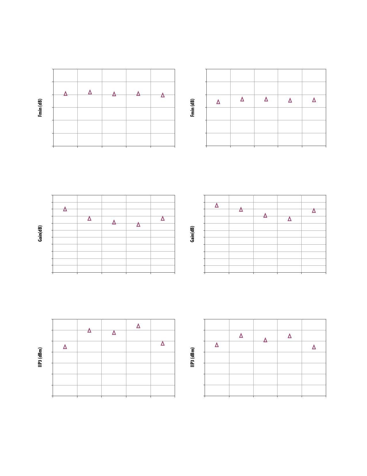
Figure 7. Fmin vs Idd at 4.8 V at 2.5 GHz
90
100
0.3
60
80 84
Idd (mA)
Figure 8. Fmin vs Idd at 4.8 V at 2 GHz
90
100
22
20
18
16
14
12
10
8
6
4
2
0
60
80 84 90
Idd (mA)
100
Figure 9. Gain vs Idd at 4.8 V Tuned for Optimum IIP3 and Fmin at 2.5 GHz
22
20
18
16
14
12
10
8
6
4
2
0
60
80 84 90
Idd (mA)
100
Figure 10. Gain vs Idd at 4.8 V Tuned for Optimum IIP3 and Fmin at 2 GHz
35
30
25
20
15
10
5
0
60
80 84 90
Idd (mA)
100
Figure 11. IIP3 vs Idd at 4.8 V Tuned for Optimum IIP3 and Fmin at 2.5 GHz
35
30
25
20
15
10
5
0
60
80 84 90
Idd (mA)
100
Figure 12. IIP3 vs Idd at 4.8 V Tuned for Optimum IIP3 and Fmin at 2 GHz
5
5 Page 
Typical Noise Parameters, Vdd = 4.8 V, Idd = 84 mA
Freq Fmin opt opt
GHz dB
Mag. Ang. Rn/50
1.9
0.656
0.193
152.8
0.044
2
0.664
0.206
156.4
0.040
2.2
0.678
0.234
163.5
0.035
2.5
0.704
0.274
174.2
0.034
2.7
0.736
0.301
181.4
0.036
3.3
0.958
0.383
202.8
0.045
3.5
1.12
0.41
209.9
0.045
Notes:
1. The Fmin values are based on noise figure measurements at 100
different impedances using Focus source pull test system. From
these measurements a true Fmin is calculated.
2. Scatteringandnoiseparametersaremeasuredoncoplanarwaveguide
made on 0.010 inch thick ROGER 4350. The input reference plane is
at the end of the RFinput pin and the output reference plane is at the
end of the RFoutput pin as shown in Figure 25.
Part Number Ordering Information
Part Number
No. of Devices
MGA-638P8-BLKG
100
MGA-638P8-TR1G
3000
Container
Antistatic Bag
7 inch Reel
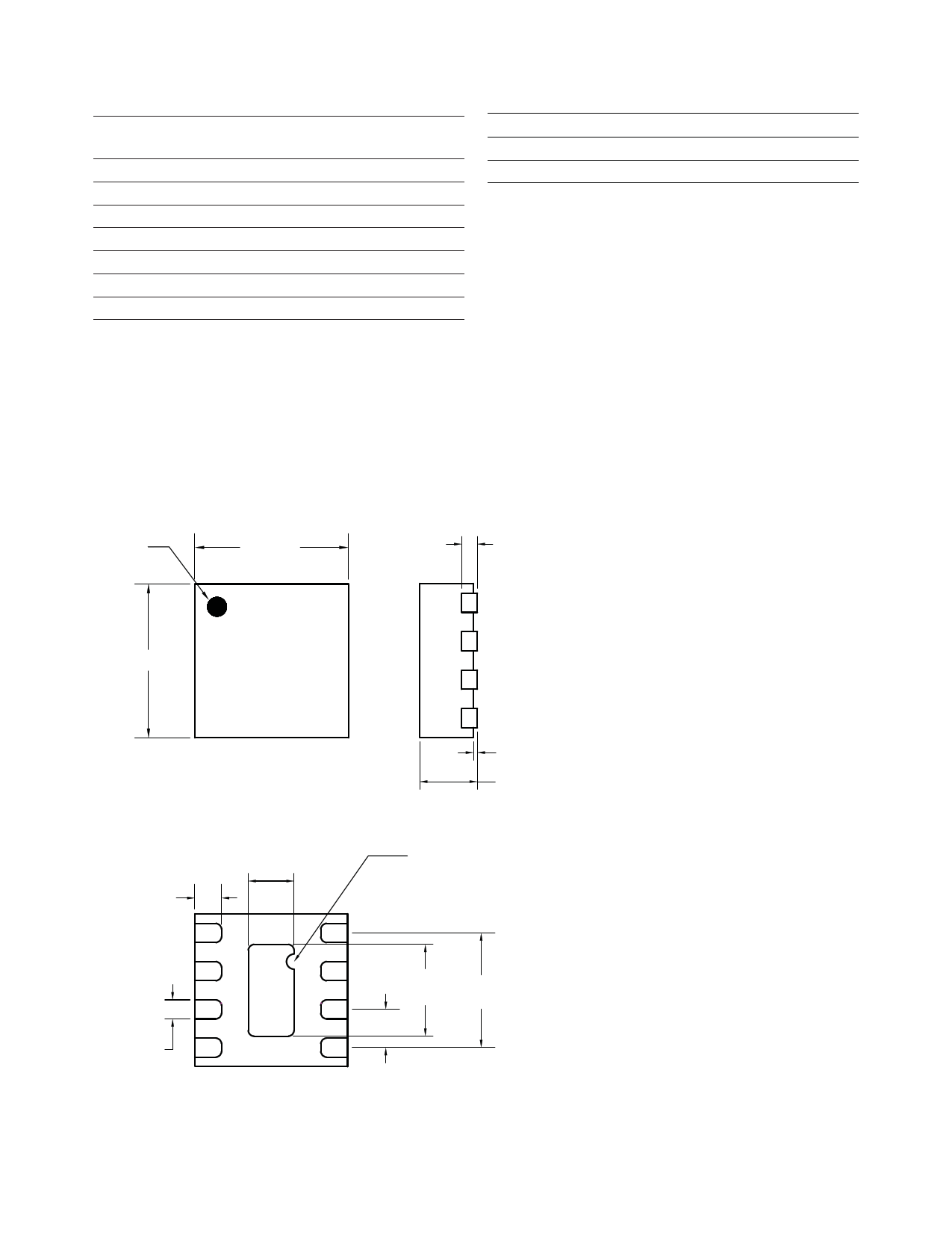
DFN2X2 Package Dimensions
PIN 1 DOT
BY MARKING
2.00±0.10
0.20 Ref.
2.00±0.10
38X
0.35±0.05
TOP VIEW
0.60±0.05
Exp. DAP
0.0–0.05
0.75±0.10
SIDE VIEW
PIN #1 IDENTIFICATION
R0.10
0.25±0.05
11
1.20±0.05
Exp. DAP
0.50 Bsc
1.50
Ref.
Notes:
1. All dimensions are in millimeters.
2. Dimensions are inclusive of plating.
3. Dimensions are exclusive of mold ash and metal burr.
BOTTOM VIEW
11 Page | ||
| Páginas | Total 14 Páginas | |
| PDF Descargar | [ Datasheet MGA-638P8.PDF ] | |
Hoja de datos destacado
| Número de pieza | Descripción | Fabricantes |
| MGA-638P8 | High Linearity Low Noise Amplifier | AVAGO |
| Número de pieza | Descripción | Fabricantes |
| SLA6805M | High Voltage 3 phase Motor Driver IC. |
Sanken |
| SDC1742 | 12- and 14-Bit Hybrid Synchro / Resolver-to-Digital Converters. |
Analog Devices |
|
DataSheet.es es una pagina web que funciona como un repositorio de manuales o hoja de datos de muchos de los productos más populares, |
| DataSheet.es | 2020 | Privacy Policy | Contacto | Buscar |
