|
|
PDF MGA-683P8 Data sheet ( Hoja de datos )
| Número de pieza | MGA-683P8 | |
| Descripción | Low Noise And High Linearity Active Bias Low Noise Amplifier | |
| Fabricantes | AVAGO | |
| Logotipo |  |
|
Hay una vista previa y un enlace de descarga de MGA-683P8 (archivo pdf) en la parte inferior de esta página. Total 11 Páginas | ||
|
No Preview Available !
MGA-683P8
Low Noise And High Linearity Active Bias
Low Noise Amplifier
Data Sheet
Description
Avago Technologies’ MGA-683P8 is an economical, easy-
to-use GaAs MMIC Low Noise Amplifier (LNA). The LNA
has low noise and high linearity achieved through the
use of Avago Technologies’ proprietary 0.25 m GaAs
Enhancement-mode pHEMT process. It is housed in a
miniature 2.0 x 2.0 x 0.75 mm3 8-pin Quad-Flat-Non-Lead
(QFN) package. It is designed for optimum use from 450
MHz up to 2 GHz. The compact footprint and low profile
coupled with low noise, high gain and high linearity make
the MGA-683P8 an ideal choice as a low noise amplifier for
cellular infrastructure for GSM and CDMA. For optimum
performance at higher frequency from 1.5 GHz to 4 GHz,
the MGA-684P8 is recommended. Both MGA-683P8 and
MGA-684P8 share the same package and pinout.
Pin Configuration and Package Marking
2.0 x 2.0 x 0.75 mm3 8-lead QFN
[1] [8]
[2] 83X [7]
[3] [6]
[4] [5]
[8]
[7]
[6]
[5]
[1]
[2]
[3]
[4]
Top View
Bottom View
Pin 1 – Vbias
Pin 2 – RFinput
Pin 3 – Not Used
Pin 4 – Not Used
Pin 5 – Not Used
Pin 6 – Not Used
Pin 7 – RFoutput/Vdd
Pin 8 – Not Used
Centre tab - Ground
Note:
Package marking provides orientation and identification
“83” = Device Code
“X” = Month Code
Features
Low noise Figure
High linearity performance
GaAs E-pHEMT Technology[1]
Low cost small package size: 2.0 x 2.0 x 0.75 mm3
Excellent uniformity in product specifications
Tape-and-Reel packaging option available
Specifications
900 MHz; 5 V, 40 mA
17.8 dB Gain
0.56 dB Noise Figure
More than 20 dB Input Return Loss
32.8 dBm Output IP3
21.5 dBm Output Power at 1dB gain compression
Applications
Low noise amplifier for cellular infrastructure for GSM
and CDMA.
Other low noise application.
Repeater, Metrocell/Picocell application.
Simplified Schematic
Vdd
C5 Rbias C6
R1
C3
R2 C4
RFin
L3
L1
C1
[1]
[2]
[3]
[4]
L2
[8] C2
[7]
[6]
[5]
RFout
Attention: Observe precautions for
handling electrostatic sensitive devices.
ESD Machine Model = 90 V (Class A)
ESD Human Body Model = 500 V (Class 1B)
Refer to Avago Application Note A004R:
Electrostatic Discharge, Damage and Control.
Note:
The schematic is shown with the assumption that similar PCB is used
for both MGA-683P8 and MGA-684P8.
Detail of the components needed for this product is shown in Table 1.
Enhancement mode technology employs positive gate voltage,
thereby eliminating the need of negative gate voltage associated
with conventional depletion mode devices.
Good RF practice requires all unused pins to be earthed.
1 page 
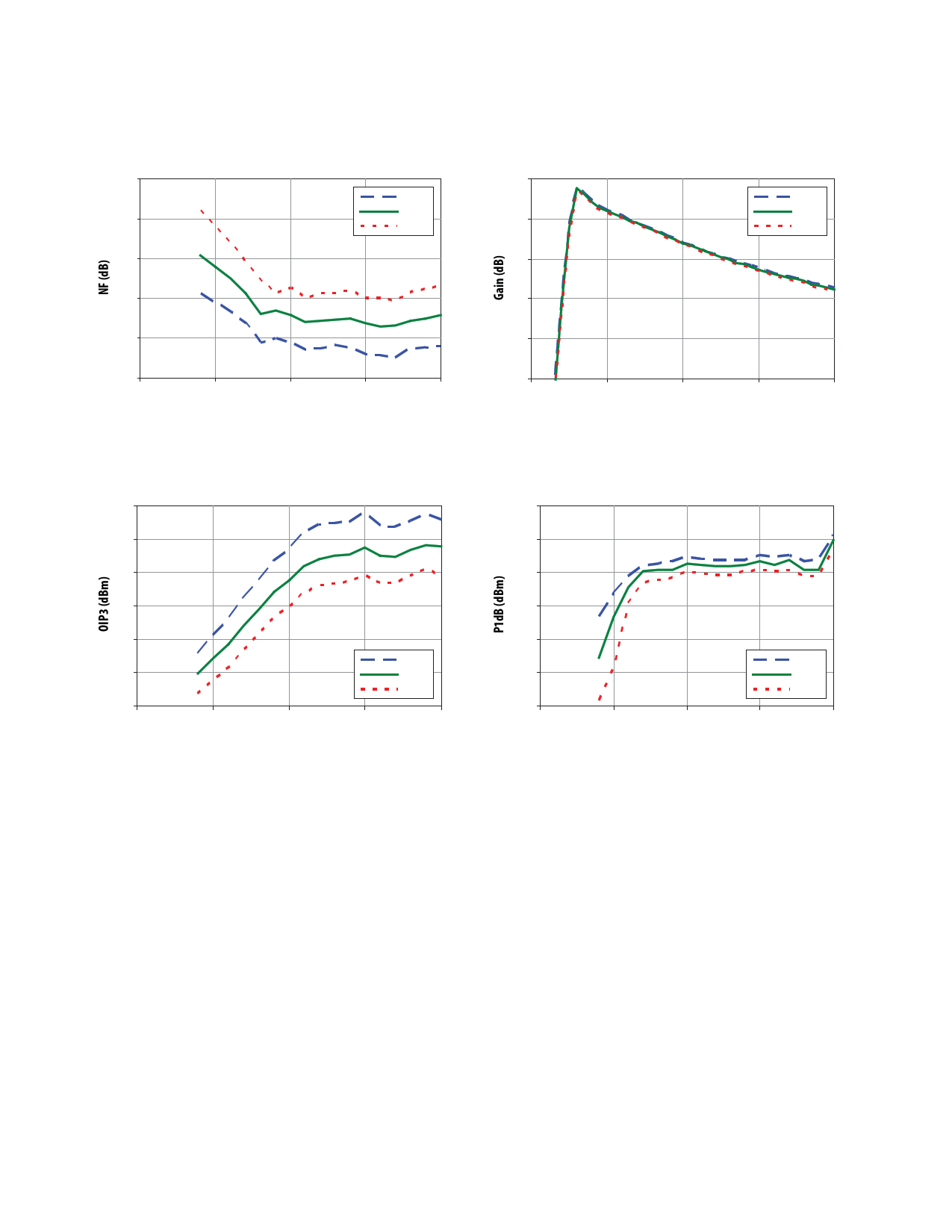
MGA-683P8 Typical Performance in Demoboard
RF performance at TA = 25° C, Vdd = 5 V, measured on demo board in Figure 5 with component list in Table1 for 900 MHz
matching, unless otherwise stated.
1.2 25
-40° C
1
25° C
85° C
20
-40° C
25° C
85° C
0.8 15
0.6 10
0.4 5
0.2
0 500 1000
Frequency (MHz)
Figure 7. NF vs Frequency vs Temperature
1500
0
2000 0 500 1000 1500
Frequency (MHz)
Figure 8. Gain vs Frequency vs Temperature
2000
38
36
34
32
30
-40° C
28 25° C
85° C
26
0 500 1000 1500 2000
Frequency (MHz)
Figure 9. OIP3 vs Frequency vs Temperature
23.5
22.5
21.5
20.5
19.5
18.5
17.5
0
500 1000
Frequency (MHz)
Figure 10. OP1dB vs Frequency vs Temperature
-40° C
25° C
85° C
1500 2000
5
5 Page 
Reel Dimensions – 7 inch
SEE DETAIL "X"
6.25mm EMBOSSED LETTERS
LETTERING THICKNESS: 1.6mm
SLOT HOLE "b"
SLOT HOLE "a"
Ø178.0±0.5
FRONT
BACK
P6S
SLOT HOLE(2x)
180° APART.
6
PS
RECYCLE LOGO
FRONT VIEW
R10.65
R5.2
65° 45°
SLOT HOLE "a": 3.0±0.5mm(1x)
SLOT HOLE "b": 2.5±0.5mm(1x)
12.4 +1.5*
-0.0
1.5 MIN.
+0.5
Ø13.0 -0.2
Ø20.2 MIN.
FRONT
BACK
DETAIL "X"
3.5
DETAIL "Y"
(Slot Hole)
EMBOSSED RIBS
RAISED: 0.25mm, WIDTH: 1.25mm
BACK VIEW
Ø178.0±0.5
Ø51.2±0.3
SEE DETAIL "Y"
18.0*
MAX.
For product information and a complete list of distributors, please go to our web site: www.avagotech.com
Avago, Avago Technologies, and the A logo are trademarks of Avago Technologies in the United States and other countries.
Data subject to change. Copyright © 2005-2011 Avago Technologies. All rights reserved.
AV02-2945EN - June 22, 2011
11 Page | ||
| Páginas | Total 11 Páginas | |
| PDF Descargar | [ Datasheet MGA-683P8.PDF ] | |
Hoja de datos destacado
| Número de pieza | Descripción | Fabricantes |
| MGA-683P8 | Low Noise And High Linearity Active Bias Low Noise Amplifier | AVAGO |
| Número de pieza | Descripción | Fabricantes |
| SLA6805M | High Voltage 3 phase Motor Driver IC. |
Sanken |
| SDC1742 | 12- and 14-Bit Hybrid Synchro / Resolver-to-Digital Converters. |
Analog Devices |
|
DataSheet.es es una pagina web que funciona como un repositorio de manuales o hoja de datos de muchos de los productos más populares, |
| DataSheet.es | 2020 | Privacy Policy | Contacto | Buscar |
