|
|
|
PDF ICX205AL Data sheet ( Hoja de datos )
| Número de pieza | ICX205AL | |
| Descripción | Diagonal 8mm (Type 1/2) Progressive Scan CCD Image Sensor | |
| Fabricantes | Sony | |
| Logotipo | ||
Hay una vista previa y un enlace de descarga de ICX205AL (archivo pdf) en la parte inferior de esta página. Total 22 Páginas | ||
|
No Preview Available !
ICX205AL
Diagonal 8mm (Type 1/2) Progressive Scan CCD Image Sensor with Square Pixel for B/W Cameras
Description
The ICX205AL is a diagonal 8mm (Type 1/2)
interline CCD solid-state image sensor with a square
pixel array and 1.45M effective pixels. Progressive
scan allows all pixels' signals to be output
independently within approximately 1/7.5 second.
Also, the adoption of high frame rate readout mode
supports 30 frames per second. This chip features
an electronic shutter with variable charge-storage
time which makes it possible to realize full-frame still
image without a mechanical shutter. High sensitivity
and low dark current are achieved through the
adoption of HAD (Hole-Accumulation Diode) sensors.
This chip is suitable for applications such as
electronic still cameras, PC input cameras, etc.
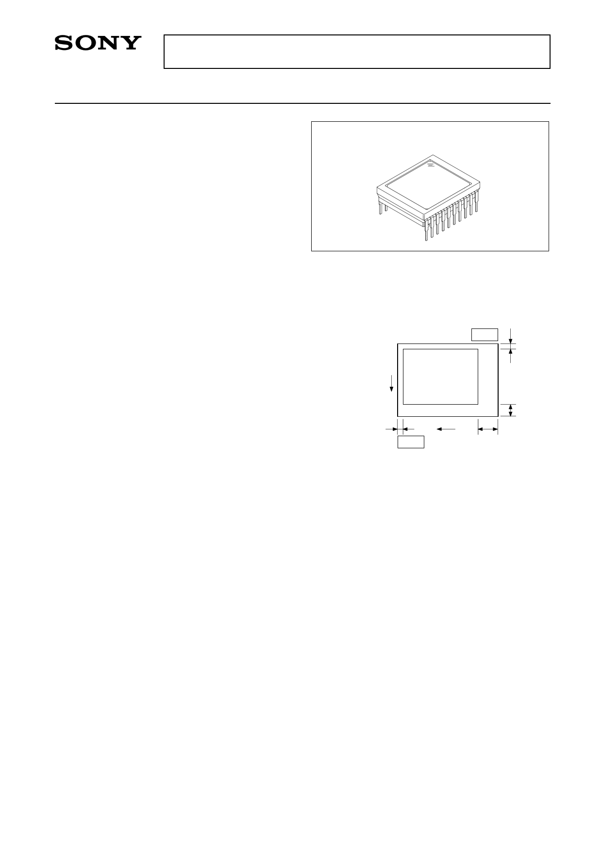
20 pin DIP (Cer-DIP)
Features
• Progressive scan allows individual readout of the
image signals from all pixels.
• High horizontal and vertical resolution (both approx.
1024TV-lines) still image without a mechanical shutter.
• Supports high frame rate readout mode
(effective 256 lines output, 30 frame/s)
• Square pixel
• Horizontal drive frequency: 14.318MHz
• No voltage adjustments
(reset gate and substrate bias are not adjusted.)
• High resolution, high sensitivity, low dark current
• Low smear, excellent antiblooming characteristics
• Continuous variable-speed shutter
Pin 1
2
V
2
Pin 11
H
40
Optical black position
(Top View)
8
Device Structure
• Interline CCD image sensor
• Image size:
• Total number of pixels:
• Number of effective pixels:
• Number of active pixels:
• Chip size:
• Unit cell size:
• Optical black:
• Number of dummy bits:
• Substrate material:
Diagonal 8mm (Type 1/2)
1434 (H) × 1050 (V) approx. 1.50M pixels
1392 (H) × 1040 (V) approx. 1.45M pixels
1360 (H) × 1024 (V) approx. 1.40M pixels (7.959mm diagonal)
7.60mm (H) × 6.20mm (V)
4.65µm (H) × 4.65µm (V)
Horizontal (H) direction: Front 2 pixels, rear 40 pixels
Vertical (V) direction: Front 8 pixels, rear 2 pixels
Horizontal 20
Vertical 3
Silicon
Sony reserves the right to change products and specifications without prior notice. This information does not convey any license by
any implication or otherwise under any patents or other right. Application circuits shown, if any, are typical examples illustrating the
operation of the devices. Sony cannot assume responsibility for any problems arising out of the use of these circuits.
–1–
E98619B29
1 page 
ICX205AL
Clock Equivalent Circuit Constant
Item
Capacitance between vertical transfer clock and
GND
Capacitance between vertical transfer clocks
Capacitance between horizontal transfer clock
and GND
Symbol
CφV1
CφV2A
CφV2B
CφV3
CφV12A, CφV2B1
CφV2A3, CφV32B
CφV13
CφH1, CφH2
Capacitance between horizontal transfer clocks CφHH
Capacitance between reset gate clock and GND CφRG
Capacitance between substrate clock and GND CφSUB
R1
Vertical transfer clock series resistor
R2A, R3
R2B
Vertical transfer clock ground resistor
RGND
Horizontal transfer clock series resistor
RφH
Reset gate clock series resistor
RφRG
Vφ1 Vφ2A
Min. Typ. Max. Unit Remarks
2200
pF
1800
pF
6800
pF
3300
pF
1200
pF
1200
pF
2200
pF
47 pF
100 pF
8 pF
680 pF
36 Ω
56 Ω
43 Ω
30 Ω
15 Ω
20 Ω
R1 CφV12A R2A
CφV2B1
CφV1
CφV2A
CφV2A3
CφV13
CφV2B RGND CφV3
R2B
CφV32B
R3
RφH
Hφ1
CφH1
CφHH
RφH
Hφ2
CφH2
Vφ2B
Vφ3
Vertical transfer clock equivalent circuit
RGφ
RφRG
Horizontal transfer clock equivalent circuit
CφRG
Reset gate clock equivalent circuit
–5–
5 Page 
ICX205AL
Measurement conditions
1) In the following measurements, the device drive conditions are at the typical values of the progressive scan
mode, bias and clock voltage conditions.
2) In the following measurements, spot blemishes are excluded and, unless otherwise specified, the optical
black level (OB) is used as the reference for the signal output, which is taken as the value measured at
point [∗B] of the measurement system.
Definition of standard imaging conditions
1) Standard imaging condition I:
Use a pattern box (luminance : 706cd/m2, color temperature of 3200K halogen source) as a subject.
(pattern for evaluation is not applicable.) Use a testing standard lens with CM500S (t = 1.0mm) as an IR cut
filter and image at F8. The luminous intensity to the sensor receiving surface at this point is defined as the
standard sensitivity testing luminous intensity.
2) Standard imaging condition II:
Image a light source (color temperature of 3200K) with a uniformity of brightness within 2% at all angles.
Use a testing standard lens with CM500S (t = 1.0mm) as an IR cut filter. The luminous intensity is adjusted
to the value indicated in each testing item by the lens diaphragm.
1. Sensitivity
Set to standard imaging condition I. After selecting the electronic shutter mode with a shutter speed of
1/250s, measure the signal output (VS) at the center of the screen, and substitute the value into the
following formula.
S
=
VS
×
250
30
[mV]
2. Saturation signal
Set to standard imaging condition II. After adjusting the luminous intensity to 10 times the intensity with the
average value of the signal output, 150mV, measure the minimum value of the signal output.
3. Smear
Set to standard imaging condition II. With the lens diaphragm at F5.6 to F8, first adjust the luminous
intensity to 500 times the intensity with the average value of the signal output, 150mV. Then after the
readout clock is stopped and the charge drain is executed by the electronic shutter at the respective H
blankings, measure the maximum value (Vsm [mV]) of the signal output and substitute the value into the
following formula.
Sm =
Vsm
150
×
1
500
×
1
10
× 100 [%] (1/10V method conversion value)
4. Video signal shading
Set to standard imaging condition II. With the lens diaphragm at F5.6 to F8, adjust the luminous intensity
so that the average value of the signal output is 150mV. Then measure the maximum (Vmax [mV]) and
minimum (Vmin [mV]) values of the signal output and substitute the values into the following formula.
SH = (Vmax – Vmin)/150 × 100 [%]
5. Dark signal
Measure the average value of the signal output (Vdt [mV]) with the device ambient temperature 60°C and
the device in the light-obstructed state, using the horizontal idle transfer level as a reference.
– 11 –
11 Page | ||
| Páginas | Total 22 Páginas | |
| PDF Descargar | [ Datasheet ICX205AL.PDF ] | |
Hoja de datos destacado
| Número de pieza | Descripción | Fabricantes |
| ICX205AK | Diagonal 8mm (Type 1/2) Progressive Scan CCD Image Sensor | Sony |
| ICX205AL | Diagonal 8mm (Type 1/2) Progressive Scan CCD Image Sensor | Sony |
| Número de pieza | Descripción | Fabricantes |
| SLA6805M | High Voltage 3 phase Motor Driver IC. |
Sanken |
| SDC1742 | 12- and 14-Bit Hybrid Synchro / Resolver-to-Digital Converters. |
Analog Devices |
|
DataSheet.es es una pagina web que funciona como un repositorio de manuales o hoja de datos de muchos de los productos más populares, |
| DataSheet.es | 2020 | Privacy Policy | Contacto | Buscar |