|
|
|
PDF L6997DTR Data sheet ( Hoja de datos )
| Número de pieza | L6997DTR | |
| Descripción | STEP DOWN CONTROLLER FOR LOW VOLTAGE OPERATIONS | |
| Fabricantes | STMicroelectronics | |
| Logotipo | ||
Hay una vista previa y un enlace de descarga de L6997DTR (archivo pdf) en la parte inferior de esta página. Total 23 Páginas | ||
|
No Preview Available !
L6997
STEP DOWN CONTROLLER
FOR LOW VOLTAGE OPERATIONS
FEATURES
s FROM 3V TO 5.5V VCC RANGE.
s MINIMUM OUTPUT VOLTAGE AS LOW AS
0.6V.
s 1V TO 28V INPUT VOLTAGE RANGE.
s CONSTANT ON TIME TOPOLOGY ALLOWS.
OPERATION WITH VERYLOW AND HIGH
DUTY CYCLES.
s VERY FAST LOAD TRANSIENTS.
s 0.6V, ±1% VREF.
s SELECTABLE SINKING MODE.
s LOSSLESS CURRENT LIMIT, AVAILABLE
ALSO IN SINKING MODE
s REMOTE SENSING.
s OVP,UVP LATCHED PROTECTIONS.
s 600µA TYP QUIESCENT CURRENT.
s POWER GOOD AND OVP SIGNALS.
s PULSE SKIPPING AT LIGTH LOADS.
s 94% EFFICIENCY FROM 3.3V TO 2.5V.
APPLICATIONS
s NETWORKING.
s DC/DC MODULES.
s DISTRIBUTED POWER.
s MOBILE APPLICATIONS.
s CHIP SET, CPU, DSP AND MEMORIES SUPPLY.
TSSOP20
ORDERING NUMBERS: L6997D
L6997DTR
DESCRIPTION
The device is a high efficient solution for networking
dc/dc modules and mobile application compatible
with 3.3V bus and 5V bus.
It's able to regulate an output voltage as low as 0.6V.
The constant on time topology assures fast load tran-
sient response. The embedded voltage feed-forward
provides nearly constant switching frequency opera-
tion.
An integrator can be introduced in the control loop to
reduce the static output voltage error.
The remote sensing improves the static and dynamic
regulation, recovering the wires voltage drop.
Pulse skipping technique reduces power consump-
tion at light loads. Drivers current capability allows
output currents in excess of 20A.
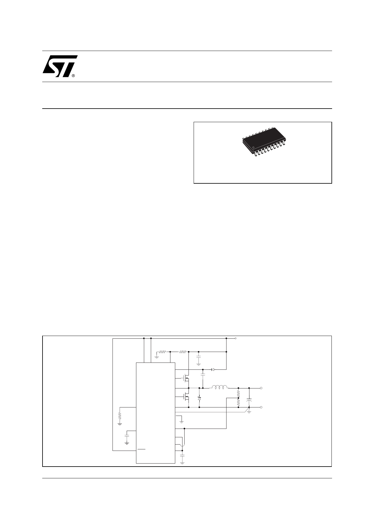
MINIMUM COMPONENT COUNT APPLICATION
Rin2
Rin1
3.3V
OSC
BOOT
HGATE
Rilim
PGOOD
PHASE
OVP
LGATE
L6997
ILIM PGND
GND
GNDSENSE
Cin
Dboot
HS Cboot
L
LS DS
0.6V
Ro1
Ro2
Cout
SS
Css
SHDN
VSENSE
INT
VFB
Vref
Cvref
April 2003
1/23
1 page 
Figure 1. Functional & Block Diagram
L6997
5/23
5 Page 
L6997
1.6 Protection and fault
Sensing VSENSE pin voltage performs output protection. The nature of the fault (that is, latched OV or latched
UV) is given by the PGOOD and OVP pins. If the output voltage is between the 89% (typ.) and 110% (typ) of
the regulated value, PGOOD is high. If a hard overvoltage or an undervoltage occurs, the device is latched: low
side MOSFET and, high side MOSFET are turned off and PGOOD goes low. In case the system detects an
overvoltage the OVP pin goes high.
To recover the functionality the device must be shut down and restarted thought the SHDN pin, or the supply
has to be removed, and restart with the correct sequence.
These features are useful to protect against short-circuit (UV fault) as well as high side MOSFET short (OV
fault).
1.7 Drivers
The integrated high-current drivers allow using different size of power MOSFET, maintaining fast switching tran-
sition. The driver for the high side MOSFET uses the BOOT pin for supply and PHASE pin for return (floating
driver). The driver for the low side MOSFET uses the VDR pin for the supply and PGND pin for the return. The
main feature is the adaptive anti-cross-conduction protection, which prevents from both high side and low side
MOSFET to be on at the same time, avoiding a high current to flow from VIN to GND. When high side MOSFET
is turned off the voltage on the pin PHASE begins to fall; the low side MOSFET is turned on only when the volt-
age on PHASE pin reaches 250mV. When low side is turned off, high side remains off until LGATE pin voltage
reaches 500mV. This is important since the driver can work properly with a large range of external power MOS-
FETS.
The current necessary to switch the external MOSFETS flows through the device, and it is proportional to the
MOSFET gate charge and the switching frequency. So the power dissipation of the device is function of the ex-
ternal power MOSFET gate charge and switching frequency.
Eq 14 Pdrive r = Vcc ⋅ Qg TOT ⋅ FSW
The maximum gate charge values for the low side and high side are given from:
Eq 15
QMAXHS
=
f--S----W-----0-
fSW
⋅
75 n
C
Eq 16
QMAXLS
=
f--S----W-----0-
fSW
⋅
125 n C
Where fSW0 = 500Khz. The equations above are valid for TJ = 150°C. If the system temperature is lower the QG
can be higher.
For the Low Side driver the max output gate charge meets another limit due to the internal traces degradation;
in this case the maximum value is QMAXLS = 125nC.
The low side driver has been designed to have a low resistance pull-down transistor, around 0.5 ohms. This
prevents the voltage on LGATE pin raises during the fast rise-time of the pin PHASE, due to the Miller effect.
Because the driver voltage can be very low it should be considered also the ULTRA LOW VOLTAGE MOSFET.
This kind of MOSFET has very low threshold voltage, so the overdrive voltage can be enough to ensure correct
transition and low enough RDSON.
11/23
11 Page | ||
| Páginas | Total 23 Páginas | |
| PDF Descargar | [ Datasheet L6997DTR.PDF ] | |
Hoja de datos destacado
| Número de pieza | Descripción | Fabricantes |
| L6997DTR | STEP DOWN CONTROLLER FOR LOW VOLTAGE OPERATIONS | STMicroelectronics |
| Número de pieza | Descripción | Fabricantes |
| SLA6805M | High Voltage 3 phase Motor Driver IC. |
Sanken |
| SDC1742 | 12- and 14-Bit Hybrid Synchro / Resolver-to-Digital Converters. |
Analog Devices |
|
DataSheet.es es una pagina web que funciona como un repositorio de manuales o hoja de datos de muchos de los productos más populares, |
| DataSheet.es | 2020 | Privacy Policy | Contacto | Buscar |