|
|
|
PDF GD25Q20 Data sheet ( Hoja de datos )
| Número de pieza | GD25Q20 | |
| Descripción | Dual and Quad SPI Flash | |
| Fabricantes | GigaDevice | |
| Logotipo | ||
Hay una vista previa y un enlace de descarga de GD25Q20 (archivo pdf) en la parte inferior de esta página. Total 30 Páginas | ||
|
No Preview Available !
Uniform Sector
Dual and Quad SPI Flash
GD25Q40/20/10/512
FEATURES
◆ 4M/2M/1M/512K-bit Serial Flash
-512/256/128/64K-byte
-256 bytes per programmable page
◆ Standard, Dual, Quad SPI
-Standard SPI: SCLK, CS#, SI, SO, WP#, HOLD#
-Dual SPI:SCLK, CS#, IO0, IO1, WP#, HOLD#
-Quad SPI:SCLK, CS#, IO0, IO1, IO2, IO3
◆ High Speed Clock Frequency
-120MHz for fast read with 30PF load
-Dual I/O Data transfer up to 240Mbits/s
-Quad I/O Data transfer up to 480Mbits/s
◆ Program/Erase Speed
-Page Program time:0.7ms typical
-Sector Erase time:150ms typical
-Block Erase time:0.3\0.5s typical
-Chip Erase time:3\2\1\0.5s typical
◆ Flexible Architecture
-Sector of 4K-byte
-Block of 32/64K-byte
◆ Low Power Consumption
-20mA maximum active current
-5uA maximum power down current
◆ Software/Hardware Write Protection
◆ Advanced security Features(1)
-Write protect all/portion of memory via software
-16-Bit Customer ID
-Enable/Disable protection with WP# Pin
-Security Architecture
-Top or Bottom, Sector or Block selection
◆ Single Power Supply Voltage
◆ Minimum 100,000 Program/Erase Cycles
-Full voltage range:2.7~3.6V
Note: 1.Please contact Gigadevice for details.
GENERAL DESCRIPTION
The GD25Q40/20/10/512 (4M-bit) SPI flash supports the standard Serial Peripheral Interface (SPI), and a high
performance Dual/Quad output as well as Dual/Quad SPI: Serial Clock, Chip Select, Serial Data I/O0 (SI), I/O1 (SO),
I/O2 (WP#), and I/O3 (HOLD#). SPI clock frequencies of up to 120MHz are supported allowing equivalent clock rates of
240MHz for Dual Output & Dual I/O read command, and 480MHz for Quad output & Quad I/O read command.
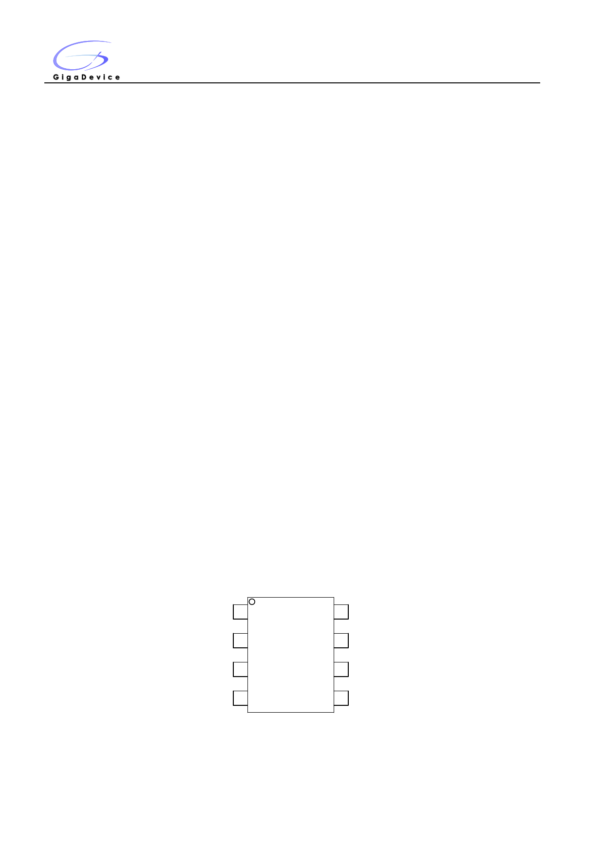
CONNECTION DIAGRAM
CS# 1
8
SO
WP#
27
Top View
36
VSS
45
8–LEAD SOP/DIP
VCC
HOLD#
SCLK
SI
1
1 page 
Uniform Sector
Dual and Quad SPI Flash
GD25Q10 64K Bytes Block Sector Architecture
Block
Sector
31
1 ……
16
15
0 ……
0
GD25Q512 32K Bytes Block Sector Architecture
Block
Sector
15
1 ……
8
7
0 ……
0
GD25Q40/20/10/512
Address range
01F000H
……
010000H
00F000H
……
000000H
01FFFFH
……
010FFFH
00FFFFH
……
000FFFH
Address range
00F000H
……
008000H
007000H
……
000000H
00FFFFH
……
008FFFH
007FFFH
……
000FFFH
5
5 Page 
Uniform Sector
Dual and Quad SPI Flash
GD25Q40/20/10/512
COMMANDS DESCRIPTION
All commands, addresses and data are shifted in and out of the device, beginning with the most significant bit on the
first rising edge of SCLK after CS# is driven low. Then, the one-byte command code must be shifted in to the device, most
significant bit first on SI, each bit being latched on the rising edges of SCLK.
See Table2, every command sequence starts with a one-byte command code. Depending on the command, this
might be followed by address bytes, or by data bytes, or by both or none. CS# must be driven high after the last bit of the
command sequence has been shifted in. For the command of Read, Fast Read, Read Status Register or Release from
Deep Power-Down, and Read Device ID, the shifted-in command sequence is followed by a data-out sequence. CS# can
be driven high after any bit of the data-out sequence is being shifted out.
For the command of Page Program, Sector Erase, Block Erase, Chip Erase, Write Status Register, Write Enable,
Write Disable or Deep Power-Down command, CS# must be driven high exactly at a byte boundary, otherwise the
command is rejected, and is not executed. That is CS# must driven high when the number of clock pulses after CS# being
driven low is an exact multiple of eight. For Page Program, if at any time the input byte is not a full byte, nothing will happen
and WEL will not be reset.
Table2. Commands
Command Name
Byte 1 Byte 2
Byte 3
Byte 4
Byte 5 Byte 6
n-Bytes
Write Enable
Write Disable
Read Status Register
Read Status Register-1
Write Status Register
Read Data
Fast Read
Dual Output
Fast Read
Dual I/O
Fast Read
Quad Output
Fast Read
Quad I/O
Fast Read
Quad I/O Word
Fast Read(7)
Continuous Read Reset
Page Program
Sector Erase
Block Erase(32K)
Block Erase(64K)(8)
Chip Erase
Program/Erase
Suspend
Program/Erase Resume
Deep Power-Down
Release From Deep
Power-Down, And
Read Device ID
Release From Deep
Power-Down
06H
04H
05H
35H
01H
03H
0BH
3BH
BBH
6BH
EBH
E7H
FFH
02 H
20H
52H
D8H
C7/60 H
75H
7AH
B9H
ABH
ABH
(S7-S0)
(S15-S8)
(S7-S0)
A23-A16
A23-A16
A23-A16
(S15-S8)
A15-A8
A15-A8
A15-A8
A23-A8(2)
A23-A16
A7-A0
M7-M0(2)
A15-A8
A23-A0
M7-M0(4)
A23-A0
M7-M0(4)
dummy(5)
dummy(6)
A23-A16
A23-A16
A23-A16
A23-A16
A15-A8
A15-A8
A15-A8
A15-A8
dummy
dummy
A7-A0
A7-A0
A7-A0
(D7-D0)
dummy
dummy
(D7-D0)(1)
A7-A0
dummy
(D7-D0)(3)
(D7-D0)(3)
A7-A0
A7-A0
A7-A0
A7-A0
D7-D0
dummy
(ID7-ID0)
(Next byte)
(D7-D0)
(D7-D0)(1)
(D7-D0)(3)
Next byte
(continuous)
(continuous)
(continuous)
(continuous)
(continuous)
(continuous)
(continuous)
(continuous)
(continuous)
(continuous)
11
11 Page | ||
| Páginas | Total 30 Páginas | |
| PDF Descargar | [ Datasheet GD25Q20.PDF ] | |
Hoja de datos destacado
| Número de pieza | Descripción | Fabricantes |
| GD25Q20 | Dual and Quad SPI Flash | GigaDevice |
| GD25Q20B | Uniform sector Dual and Quad Serial Flash | GigaDevice |
| GD25Q21B | Uniform Sector Dual and Quad Serial Flash | ELM |
| GD25Q21B | Uniform Sector Dual and Quad Serial Flash | GigaDevice |
| Número de pieza | Descripción | Fabricantes |
| SLA6805M | High Voltage 3 phase Motor Driver IC. |
Sanken |
| SDC1742 | 12- and 14-Bit Hybrid Synchro / Resolver-to-Digital Converters. |
Analog Devices |
|
DataSheet.es es una pagina web que funciona como un repositorio de manuales o hoja de datos de muchos de los productos más populares, |
| DataSheet.es | 2020 | Privacy Policy | Contacto | Buscar |