|
|
|
PDF MLX75030 Data sheet ( Hoja de datos )
| Número de pieza | MLX75030 | |
| Descripción | Universal Active Light Sensor Interface | |
| Fabricantes | Melexis | |
| Logotipo | ||
Hay una vista previa y un enlace de descarga de MLX75030 (archivo pdf) en la parte inferior de esta página. Total 30 Páginas | ||
|
No Preview Available !
MLX75030
Universal Active Light Sensor Interface
Features & Benefits
Two independent simultaneously operating
active light measurement channels
Integrated DC light cancellation circuitry for
active light channel DC light suppression
Two logarithmic ambient light channels
High input capacitance tolerant input current
terminals
Extremely high degree of adaptability for
different optical systems
Stand-by and sleep modes
Integrated 16Bit ADC
Integrated temperature sensor
Easy digital communication interface via SPI
Integrated watchdog timer
High safety design by comprehensive
diagnostic and monitoring functions
Minimum amount of external components
Small-size SMD package QFN24 4x4 mm
Ordering Information
Part No.
MLX75030
MLX75030
Temperature Code
R (-40°C to 105°C)
C (0°C to 70°C)
Package Code
LQ (QFN24 4x4)
LQ (QFN24 4x4)
Option code
B
B
Application Examples
Optical proximity sensing & display dimming
Touch-less gesture recognition,
Driver/passenger discrimination
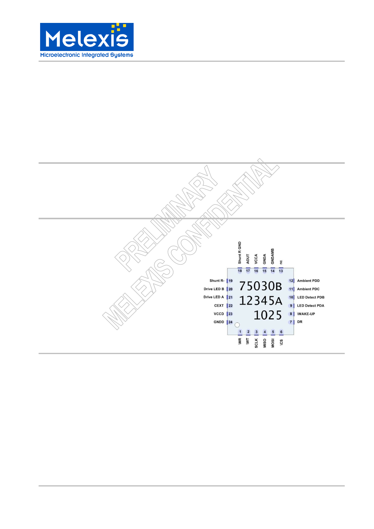
Pin Description – Top View
General Description
The MLX75030 Universal Active Light Sensor Interface was designed to allow easy and robust dual-channel
optical reflection and dual channel ambient light measurement. Therefore it is ideally suited for the design of
responsive human-machine interfaces (HMI) that require proximity or gesture detection in environments
subject to wide background light level variations, possibly in combination with display dimming.
The MLX75030 IC consists of two optical sensor interface parts. Part one is optimized for active light
measurements and is designed to control up to 2 external LEDs and to sense modulated light current from up
to 2 external photodiodes on independent channels A and B. The active light detection is virtually
independent from background light by means of integrated hardware-level ambient light suppression. Part
two consists of two logarithmic current sensors C and D, which can measure the photocurrent of externally
connected photodiodes. Simple and programmable operation is ensured by internal control logic,
configurable user registers and SPI communication.
_____75030
Rev 003
Page 1 of 58
Dec/12
Datasheet
1 page 
MLX75030
Universal Active Light Sensor Interface
Table of Contents
Functional Block Diagram ......................................................................................................................................................................... 2
1 General Description ............................................................................................................................................................................... 3
2 Glossary of Terms ................................................................................................................................................................................. 6
3 Absolute Maximum Ratings ................................................................................................................................................................... 7
4 Pin Definitions & Descriptions ................................................................................................................................................................ 7
5 General Electrical Specifications.......................................................................................................................................................... 10
6 Sensor Specific Specifications ............................................................................................................................................................. 11
7 Detailed General Description ............................................................................................................................................................... 15
7.1 Analog Sensor Functions ............................................................................................................................................................. 15
7.1.1 Active Light Sensor ............................................................................................................................................................... 15
7.1.1.1 Active Light Channel DC Light Measurement................................................................................................................. 15
7.1.2 Ambient Light Sensor............................................................................................................................................................ 15
7.1.2.1 Normal Operation .......................................................................................................................................................... 15
7.1.2.2 Diagnostics Mode Operation.......................................................................................................................................... 16
7.1.3 Temperature Sensor ............................................................................................................................................................. 16
7.1.4 DAC ...................................................................................................................................................................................... 16
7.1.5 LED Driver ............................................................................................................................................................................ 17
7.2 SPI ............................................................................................................................................................................................... 17
7.2.1 General Description of SPI Interface ..................................................................................................................................... 17
7.2.2 Detailed Explanation of SPI Instruction Words ...................................................................................................................... 21
7.2.2.1 NOP – Idle Command.................................................................................................................................................... 21
7.2.2.2 CR – Chip Reset Command........................................................................................................................................... 21
7.2.2.3 RSLP/CSLP – Request Sleep/Confirm Sleep................................................................................................................. 21
7.2.2.4 RSTBY/CSTBY - Request Standby/Confirm Standby .................................................................................................... 22
7.2.2.5 NRM – Normal Running Mode ....................................................................................................................................... 22
7.2.2.6 SM – Start Measurement ............................................................................................................................................... 22
7.2.2.7 RO – Start Read-Out ..................................................................................................................................................... 24
7.2.2.8 SM+RO - Start Measurement combined with Read-Out................................................................................................. 27
7.2.2.9 WR/RR – Write/Read Register....................................................................................................................................... 28
7.2.2.10 SD – Start Diagnostics................................................................................................................................................. 29
7.3 Internal Status Flags .................................................................................................................................................................... 31
7.4 User Registers Overview .............................................................................................................................................................. 33
7.4.1 SetAna register ..................................................................................................................................................................... 34
7.4.2 SetAH register....................................................................................................................................................................... 35
7.4.3 SetAL register ....................................................................................................................................................................... 35
7.4.4 SetBH register....................................................................................................................................................................... 36
7.4.5 SetBL register ....................................................................................................................................................................... 36
7.4.6 SetPF register....................................................................................................................................................................... 37
7.4.7 Err register ............................................................................................................................................................................ 38
7.4.8 Rst register ........................................................................................................................................................................... 39
7.4.9 GainBuf register .................................................................................................................................................................... 40
7.4.10 Calib1/Calib2 register.......................................................................................................................................................... 41
7.4.11 EnChan register .................................................................................................................................................................. 45
7.4.12 Tamb register...................................................................................................................................................................... 46
7.5 Window Watchdog Timer ............................................................................................................................................................. 47
7.6 Reset Behaviour........................................................................................................................................................................... 49
7.7 Wake-up from Sleep or Standby................................................................................................................................................... 50
7.8 CRC Calculation........................................................................................................................................................................... 51
7.9 Global Timing Diagrams ............................................................................................................................................................... 52
8 Performance Graphs ........................................................................................................................................................................... 53
8.1 LED Channel DC Measurement ................................................................................................................................................... 53
8.2 Temperature Sensor Characteristics ............................................................................................................................................ 53
8.3 Ambient Light Channel C.............................................................................................................................................................. 53
8.4 Ambient Light Channel D.............................................................................................................................................................. 53
9 Application Information ........................................................................................................................................................................ 54
9.1 Application circuit for typ. active light channel and two ambient channels ..................................................................................... 54
10 Application Comments ....................................................................................................................................................................... 55
11 Standard information regarding manufacturability of Melexis products with different soldering processes .......................................... 56
12 ESD Precautions ............................................................................................................................................................................... 57
13 Package Information.......................................................................................................................................................................... 57
14 Disclaimer.......................................................................................................................................................................................... 58
_____75030
Rev 003
Page 5 of 58
Dec/12
Datasheet
5 Page 
MLX75030
Universal Active Light Sensor Interface
6 Sensor Specific Specifications
DC Operating Parameters TA = -40°C to 105°C, TA = 0°C to 70°C (C version), VDD = 3.0V to 3.6V
(unless otherwise specified)
Active Light Channels (Detectors A & B)
Parameter
Symbol
Test Conditions
Min Typ Max Units
Active light signal optical
transfer ratio
OTR
I LED
I PDAB
30 80000
dc sunlight signal
ISun
140 900 uA
fast full scale transition at Isunmax tsunrise
3.5 ms
min. relative active light
modulation
(referred to received IR signal)
I PDAB _ min
I PDAB
- 400Hz BW,
- max LED current of 1000mA
- 25°C
- dc sun constant
- Active light response per
channel 2.5ms
0.3 %
Error condition Err6
Critical error detected on TIA output, is TIA output outside 1.1V+/- (0.65 … 0.75V)
Note: Critical error may occur if the referring active light Channel is disabled and the according diagnostic function is
enabled (see EnChan register).
Critical error may occur after enabling of the referring active light Channel due to analog settling time.
Table 4 : Active light sensor channels specifications
_____75030
Rev 003
Page 11 of 58
Dec/12
Datasheet
11 Page | ||
| Páginas | Total 30 Páginas | |
| PDF Descargar | [ Datasheet MLX75030.PDF ] | |
Hoja de datos destacado
| Número de pieza | Descripción | Fabricantes |
| MLX75030 | Universal Active Light Sensor Interface | Melexis |
| MLX75031 | Optical Gesture & Proximity Sensing IC | Melexis |
| Número de pieza | Descripción | Fabricantes |
| SLA6805M | High Voltage 3 phase Motor Driver IC. |
Sanken |
| SDC1742 | 12- and 14-Bit Hybrid Synchro / Resolver-to-Digital Converters. |
Analog Devices |
|
DataSheet.es es una pagina web que funciona como un repositorio de manuales o hoja de datos de muchos de los productos más populares, |
| DataSheet.es | 2020 | Privacy Policy | Contacto | Buscar |