|
|
|
PDF A3983 Data sheet ( Hoja de datos )
| Número de pieza | A3983 | |
| Descripción | DMOS Microstepping Driver | |
| Fabricantes | Allegro MicroSystems | |
| Logotipo | ||
Hay una vista previa y un enlace de descarga de A3983 (archivo pdf) en la parte inferior de esta página. Total 13 Páginas | ||
|
No Preview Available !
A3983
DMOS Microstepping Driver with Translator
Features and Benefits
▪ Low RDS(ON) outputs
▪ Automatic current decay mode detection/selection
▪ Mixed and Slow current decay modes
▪ Synchronous rectification for low power dissipation
▪ Internal UVLO and thermal shutdown circuitry
▪ Crossover-current protection
Package: 24-pin TSSOP with exposed thermal pad
(suffix LP)
Not to scale
Description
The A3983 is a complete microstepping motor driver with
built-in translator for easy operation. It is designed to operate
bipolar stepper motors in full-, half-, quarter-, and eighth-step
modes, with an output drive capacity of up to 35 V and ±2 A.
The A3983 includes a fixed off-time current regulator which
has the ability to operate in Slow or Mixed decay modes.
The translator is the key to the easy implementation of the
A3983. Simply inputting one pulse on the STEP input drives
the motor one microstep. There are no phase sequence tables,
high frequency control lines, or complex interfaces to program.
The A3983 interface is an ideal fit for applications where a
complex microprocessor is unavailable or is overburdened.
The chopping control in the A3983 automatically selects the
current decay mode (Slow or Mixed). When a signal occurs at
the STEP input pin, the A3983 determines if that step results
in a higher or lower current in each of the motor phases. If
the change is to a higher current, then the decay mode is set to
Slow decay. If the change is to a lower current, then the current
decay is set to Mixed (set initially to a fast decay for a period
amounting to 31.25% of the fixed off-time, then to a slow
decay for the remainder of the off-time). This current decay
Continued on the next page…
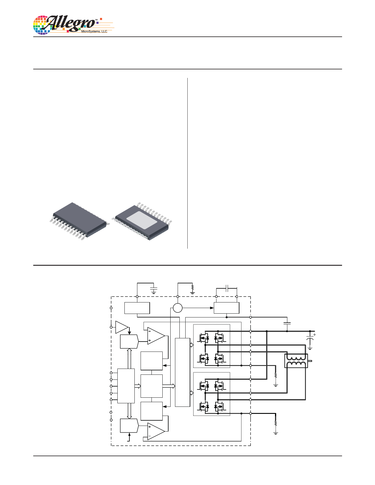
Functional Block Diagram
VREG
0.22 μF
ROSC
0.1 μF
CP1 CP2
VDD
Current
Regulator
OSC
Charge
Pump
VCP
REF
DAC
STEP
DIR
RESET
MS1
MS2
Translator
ENABLE
SLEEP
DAC
PWM Latch
Blanking
Mixed Decay
Control
Logic
PWM Latch
Blanking
Mixed Decay
DMOS Full Bridge
Gate
Drive
DMOS Full Bridge
VBB1
OUT1A
OUT1B
SENSE1
VBB2
OUT2A
OUT2B
SENSE2
VREF
0.1 μF
RS1
RS2
26184.29D
1 page 
A3983
DMOS Microstepping Driver with Translator
Functional Description
Device Operation. The A3983 is a complete microstep-
ping motor driver with a built-in translator for easy operation
with minimal control lines. It is designed to operate bipolar
stepper motors in full-, half-, quarter-, and sixteenth-step
modes. The currents in each of the two output full-bridges
and all of the N-channel DMOS FETs are regulated with
fixed off-time PMW (pulse width modulated) control cir-
cuitry. At each step, the current for each full-bridge is set by
the value of its external current-sense resistor (RS1 or RS2), a
reference voltage (VREF), and the output voltage of its DAC
(which in turn is controlled by the output of the translator).
At power-on or reset, the translator sets the DACs and the
phase current polarity to the initial Home state (shown in fig-
ures 2 through 5), and the current regulator to Mixed Decay
Mode for both phases. When a step command signal occurs
on the STEP input, the translator automatically sequences the
DACs to the next level and current polarity. (See table 2 for
the current-level sequence.) The microstep resolution is set
by the combined effect of inputs MS1 and MS2, as shown in
table 1.
When stepping, if the new output levels of the DACs are
lower than their previous output levels, then the decay mode
for the active full-bridge is set to Mixed. If the new output
levels of the DACs are higher than or equal to their previous
levels, then the decay mode for the active full-bridge is set
to Slow. This automatic current decay selection improves
microstepping performance by reducing the distortion of
the current waveform that results from the back EMF of the
motor.
RESET Input (RESET). The RESET input sets the
translator to a predefined Home state (shown in figures 2
through 5), and turns off all of the DMOS outputs. All STEP
inputs are ignored until the RESET input is set to high.
Step Input (STEP). A low-to-high transition on the STEP
input sequences the translator and advances the motor one
increment. The translator controls the input to the DACs and
the direction of current flow in each winding. The size of
the increment is determined by the combined state of inputs
MS1 and MS2.
Microstep Select (MS1 and MS2). Selects the micro-
stepping format, as shown in table 1. MS2 has a 100 kΩ pull-
down resistance. Any changes made to these inputs do not take
effect until the next STEP rising edge.
Direction Input (DIR). This determines the direction of
rotation of the motor. When low, the direction will be clock-
wise and when high, counterclockwise. Changes to this input
do not take effect until the next STEP rising edge.
Internal PWM Current Control. Each full-bridge is
controlled by a fixed off-time PWM current control circuit
that limits the load current to a desired value, ITRIP. Ini-
tially, a diagonal pair of source and sink DMOS outputs are
enabled and current flows through the motor winding and
the current sense resistor, RSx. When the voltage across RSx
equals the DAC output voltage, the current sense compara-
tor resets the PWM latch. The latch then turns off either the
source DMOS FETs (when in Slow Decay Mode) or the sink
and source DMOS FETs (when in Mixed Decay Mode).
The maximum value of current limiting is set by the selec-
tion of RSx and the voltage at the VREF pin. The transcon-
ductance function is approximated by the maximum value of
current limiting, ITripMAX (A), which is set by
ITripMAX = VREF / ( 8 RS)
where RS is the resistance of the sense resistor (Ω) and VREF
is the input voltage on the REF pin (V).
The DAC output reduces the VREF output to the current
sense comparator in precise steps, such that
×Itrip = (%ITripMAX / 100) ITripMAX
(See table 2 for %ITripMAX at each step.)
It is critical that the maximum rating (0.5 V) on the SENSE1
and SENSE2 pins is not exceeded.
Fixed Off-Time. The internal PWM current control cir-
cuitry uses a one-shot circuit to control the duration of time
that the DMOS FETs remain off. The one shot off-time, tOFF,
is determined by the selection of an external resistor con-
nected from the ROSC timing pin to ground. If the ROSC
Allegro MicroSystems, LLC
5
115 Northeast Cutoff, Box 15036
Worcester, Massachusetts 01615-0036 (508) 853-5000
www.allegromicro.com
5 Page 
A3983
DMOS Microstepping Driver with Translator
Package LP
CP1 1
CP2 2
VCP 3
VREG 4
MS1 5
MS2 6
RESET 7
ROSC 8
SLEEP 9
VDD 10
STEP 11
REF 12
PAD
24 GND
23 ENABLE
22 OUT2B
21 VBB2
20 SENSE2
19 OUT2A
18 OUT1A
17 SENSE1
16 VBB1
15 OUT1B
14 DIR
13 GND
Terminal List Table
Name
Number
Package LP
Description
CP1 1 Charge pump capacitor terminal
CP2 2 Charge pump capacitor terminal
VCP
3 Reservoir capacitor terminal
VREG
4 Regulator decoupling terminal
MS1
5 Logic input
MS2
6 Logic input
RESET
7 Logic input
ROSC
8 Timing set
SLEEP
9 Logic input
VDD
10 Logic supply
STEP
11 Logic input
REF
GND
12
13, 24
Gm reference voltage input
Ground*
DIR 14 Logic input
OUT1B
15 DMOS Full Bridge 1 Output B
VBB1
16 Load supply
SENSE1
17 Sense resistor terminal for Bridge 1
OUT1A
18 DMOS Full Bridge 1 Output A
OUT2A
19 DMOS Full Bridge 2 Output A
SENSE2
20 Sense resistor terminal for Bridge 2
VBB2
21 Load supply
OUT2B
22 DMOS Full Bridge 2 Output B
ENABLE
23 Logic input
NC – No connection
PAD
– Exposed pad for enhanced thermal dissipation*
*The GND pins must be tied together externally by connecting to the PAD ground plane
under the device.
Allegro MicroSystems, LLC
11
115 Northeast Cutoff, Box 15036
Worcester, Massachusetts 01615-0036 (508) 853-5000
www.allegromicro.com
11 Page | ||
| Páginas | Total 13 Páginas | |
| PDF Descargar | [ Datasheet A3983.PDF ] | |
Hoja de datos destacado
| Número de pieza | Descripción | Fabricantes |
| A3980 | Automotive DMOS Microstepping Driver with Translator | Allegro MicroSystems |
| A3980KLP | Automotive DMOS Microstepping Driver with Translator | Allegro MicroSystems |
| A3982 | DMOS Stepper Motor Driver | Allegro |
| A3983 | DMOS Microstepping Driver | Allegro MicroSystems |
| Número de pieza | Descripción | Fabricantes |
| SLA6805M | High Voltage 3 phase Motor Driver IC. |
Sanken |
| SDC1742 | 12- and 14-Bit Hybrid Synchro / Resolver-to-Digital Converters. |
Analog Devices |
|
DataSheet.es es una pagina web que funciona como un repositorio de manuales o hoja de datos de muchos de los productos más populares, |
| DataSheet.es | 2020 | Privacy Policy | Contacto | Buscar |