|
|
PDF CXA3741AUR Data sheet ( Hoja de datos )
| Número de pieza | CXA3741AUR | |
| Descripción | High-speed Buffer Amplifier | |
| Fabricantes | Sony | |
| Logotipo |  |
|
Hay una vista previa y un enlace de descarga de CXA3741AUR (archivo pdf) en la parte inferior de esta página. Total 15 Páginas | ||
|
No Preview Available !
High-speed Buffer Amplifier for CCD Image Sensor
CXA3741AUR
Description
The CXA3741UR is a high-speed buffer amplifier IC with built-in switches.
(Applications: CCD image sensor output buffers, digital still cameras, camcorders, other general buffers)
Features
Power consumption: 26 mW (typ.)
(IDRV = 50μA (220kΩ when VCC = 15V), ISF current = 0, during no signal)
Push-pull output
High-speed response: 500 V/μs (IDRV = 50μA (220kΩ when VCC = 15V), CL = 20pF)
Internal sink current mode for CCD source follower output. Settable by external resistance RISF
Sink current and drive current with each built-in switch. Each current value can be set by an external
resistance.
Structure
Bipolar silicon monolithic IC
Absolute Maximum Ratings
(Ta = 25°C)
Supply voltage
Input voltage
Storage temperature
Allowable power dissipation
VCC 16
V
IN
GND – 0.3 to VCC + 0.3
V
Tstg
–65 to +150
°C
PD 0.73 W
(when mounted on a two-layer board; 30mm × 30mm, t = 0.8mm)
Recommended Operating Conditions
Supply voltage
Operating temperature
VCC
Ta
9 to 15.5
–20 to +75
V
°C
Sony reserves the right to change products and specifications without prior notice. This information does not convey any license
by any implication or otherwise under any patents or other right. Application circuits shown, if any, are typical examples illustrating
the operation of the devices. Sony cannot assume responsibility for any problems arising out of the use of these circuits.
-1-
E07711
1 page 
CXA3741AUR
Electrical Characteristics
(Ta = 25°C, VCC = 15V, RIDRV0 = 220kΩ, RIDRV1 = 470kΩ, ISF0 and ISF1 pins: connected to GND)
Item
Supply current
Voltage gain
I/O offset voltage
I/O voltage range
Input bias current
Sink current
Switch control voltage
“High”
Switch control voltage
“Low”
Symbol
ICC
VGAIN
VOFFSET
VRANGE
IBIAS
ISINK
Measurement
conditions
IN = 10V,
RDRV0 = 220kΩ,
RDRV1 = 470kΩ
DRVCNT = 0V
*1
IN: F10Vdc ΔV = 1V
GAIN = ΔOUT/ΔV
IN = 10V
VOFFSET = OUT-IN
RIDRV = 100kΩ
RIDRV = 150kΩ
RIDRV = 220kΩ
RIDRV = 330kΩ
IN = 10V,
ISF0, 1 = 0V,
IDRV0, 1 = 220kΩ
IN = 10V,
ISF0, 1, IDRV0, 1 = 0V
IN = 10V,
RISF0 = 220kΩ,
RISF1 = 470kΩ
SFCNT = 0V
VcontH
VcontL
VDD = 3.0 ± 0.3V
Min.
1.5
—
–100
3.3
2.9
2.5
2.1
–6.0
3.0
2.6
2.025
—
Typ. Max.
1.7 1.9
0.999
—
— 100
— VCC – 2.0
— VCC – 1.85
— VCC – 1.8
— VCC – 1.7
3.0 20
9.0 15
2.9 3.2
——
— 0.825
Unit
mA
V/V
mV
V
μA
μA
mA
V
V
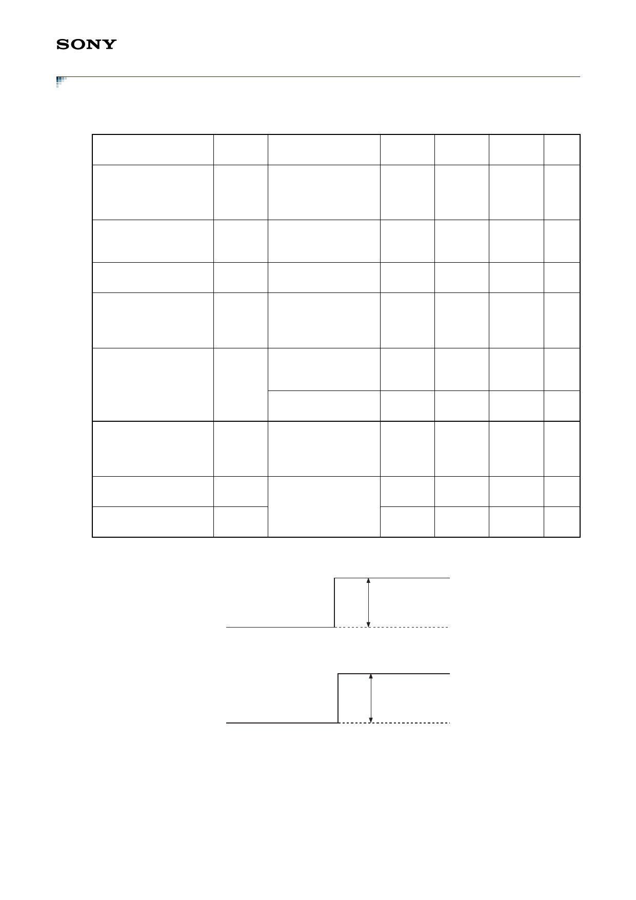
*1 Voltage gain
10.5V
IN ΔV = 1V
9.5V
OUT
ΔOUT
-5-
5 Page 
CXA3741AUR
Tr and Tf vs. Supply voltage
6.0
5.0
4.0
Tf
3.0
Tr
2.0
1.0
0
10.0
Ta = 25˚C, RIDRV = 220kΩ,
CL = 20pF, RL = 15Ω,
Input DC offset = VCC – 5V,
Input amplitude = 1.0V,
Input rise, fall time = 2.0ns
11.0 12.0 13.0 14.0 15.0
Supply voltage [V]
16.0
Tr and Tf vs. Operating temperature
4.0
3.5
Tf
3.0
Tr
2.5
2.0
1.5
1.0
0.5
0
–50
VCC = 15V, RIDRV = 220kΩ,
CL = 20pF, RL = 15Ω,
Input DC offset = VCC – 5V,
Input amplitude = 1.0V,
Input rise, fall time = 2.0ns
–25 0 25 50 75
Operating temperature [˚C]
100
I/O delay time vs. Supply voltage
2.00
1.75
1.50
1.25
1.00
0.75
0.50
0.25
0
10.0
Ta = 25˚C, RIDRV = 220kΩ,
CL = 20pF, RL = 15Ω,
Input DC offset = VCC – 5V,
Input amplitude = 1.0V,
Input rise, fall time = 2.0ns
11.0 12.0 13.0 14.0 15.0
Supply voltage [V]
16.0
I/O delay time vs. Operating temperature
2.00
1.75
1.50
VCC = 15V, RIDRV = 220kΩ,
CL = 20pF, RL = 15Ω,
Input DC offset = VCC – 5V,
Input amplitude = 1.0V,
Input rise, fall time = 2.0ns
1.25
1.00
0.75
0.50
0.25
0
–50
–25 0 25 50 75
Operating temperature [˚C]
100
Positive pulse response
10.0V
Input
T
T Output
VCC = 15V,
RIDRV = 220kΩ, CL = 20pF, RL = 15Ω
Input rise, fall time = 2.0ns
Ch1 200mVΩ Ch2 200mVΩ M 1.00ns Ch1 10.0V
1.0ns/div
10.0V
Negative pulse response
VCC = 15V,
RIDRV = 220kΩ, CL = 20pF, RL = 15Ω
Input rise, fall time = 2.0ns
T
Output
T
Input
Ch1 200mVΩ Ch2 200mVΩ M 1.00ns Ch1 10.0V
1.0ns/div
- 11 -
11 Page | ||
| Páginas | Total 15 Páginas | |
| PDF Descargar | [ Datasheet CXA3741AUR.PDF ] | |
Hoja de datos destacado
| Número de pieza | Descripción | Fabricantes |
| CXA3741AUR | High-speed Buffer Amplifier | Sony |
| Número de pieza | Descripción | Fabricantes |
| SLA6805M | High Voltage 3 phase Motor Driver IC. |
Sanken |
| SDC1742 | 12- and 14-Bit Hybrid Synchro / Resolver-to-Digital Converters. |
Analog Devices |
|
DataSheet.es es una pagina web que funciona como un repositorio de manuales o hoja de datos de muchos de los productos más populares, |
| DataSheet.es | 2020 | Privacy Policy | Contacto | Buscar |
