|
|
|
PDF OV7449 Data sheet ( Hoja de datos )
| Número de pieza | OV7449 | |
| Descripción | CMOS NTSC/PAL CAMERACHIP Sensor | |
| Fabricantes | OmniVision Technologies | |
| Logotipo | ||
Hay una vista previa y un enlace de descarga de OV7449 (archivo pdf) en la parte inferior de esta página. Total 30 Páginas | ||
|
No Preview Available !
Omni ision
®
Advanced Information
Preliminary Datasheet
OV7949/OV7449 CMOS NTSC/PAL CAMERACHIPTM Sensor
with OmniPixel® Technology for Automotive Applications
General Description
The OV7949 (color) and OV7449 (B&W) single chip
CMOS CAMERACHIP™ image sensors are designed to
provide a high level of functionality for applications
requiring a small footprint, low voltage, low power
consumption and high performance color video camera.
The OV7949 supports NTSC/PAL composite video output
and can directly interface with a VCR TV monitor or other
device with 75 ohm loading.
Note: The OV7949 is available in a
Pb lead-free package.
Features
• Single chip 1/3" format video camera
• Composite video (NTSC/PAL) differential output
drive
• Sensitivity boost (+42 dB)
• Automatic exposure/gain with 16 zone control
• Auto white balance control
• Aperture/Gamma correction
• 50/60 Hz flicker cancellation
• External frame sync capability
• SPI/EEPROM used to control overlay and set other
customer variables
• I2C compatible Serial Camera Control Bus (SCCB)
control interface for register programming
• Low power consumption
• Extremely low dark current for high temperature
applications
• Defective pixel correction
• Genlock
• QFP parts qualified to AEC-Q100 standard
Ordering Information
Product
OV07949-Q10V (Color, NTSC)
OV07449-Q10V (B&W, NTSC)
OV07949-Q20V (Color, PAL)
OV07449-Q20V (B&W, PAL)
Package
QFP-48
QFP-48
QFP-48
QFP-48
Applications
• Automobile applications
– Occupant sensor
– Adaptive cruise control
– Rear view / backup camera
– Lane departure warning
– Blind spot detection
– Night vision
Key Specifications
Array Size
Power Supply
PAL
NTSC
Analog/ADC/IO
Digital Core
Power Consumption
Image Area
Exposure Time Range
Sensitivity
S/N Ratio
Dynamic Range
Pixel Size
Dark Current
Fixed Pattern Noise
Package Dimensions
628 x 586
510 x 496
3.3 VDC + 5%
1.8 VDC + 5%
168 mW
(DVDD=1.8V,
all other voltages=3.3V,
75Ω loading)
5.961 mm x 4.276 mm
1/60s - 12 µs (NTSC)
1/50s - 12.5 µs (PAL)
4.7 V/Lux-sec @ 5600K
48 dB
50 dB
9.2 µm x 7.2 µm
10 mW/s @ 60°C
0.079% of VPEAK-TO-PEAK
14.22 mm x 14.22 mm
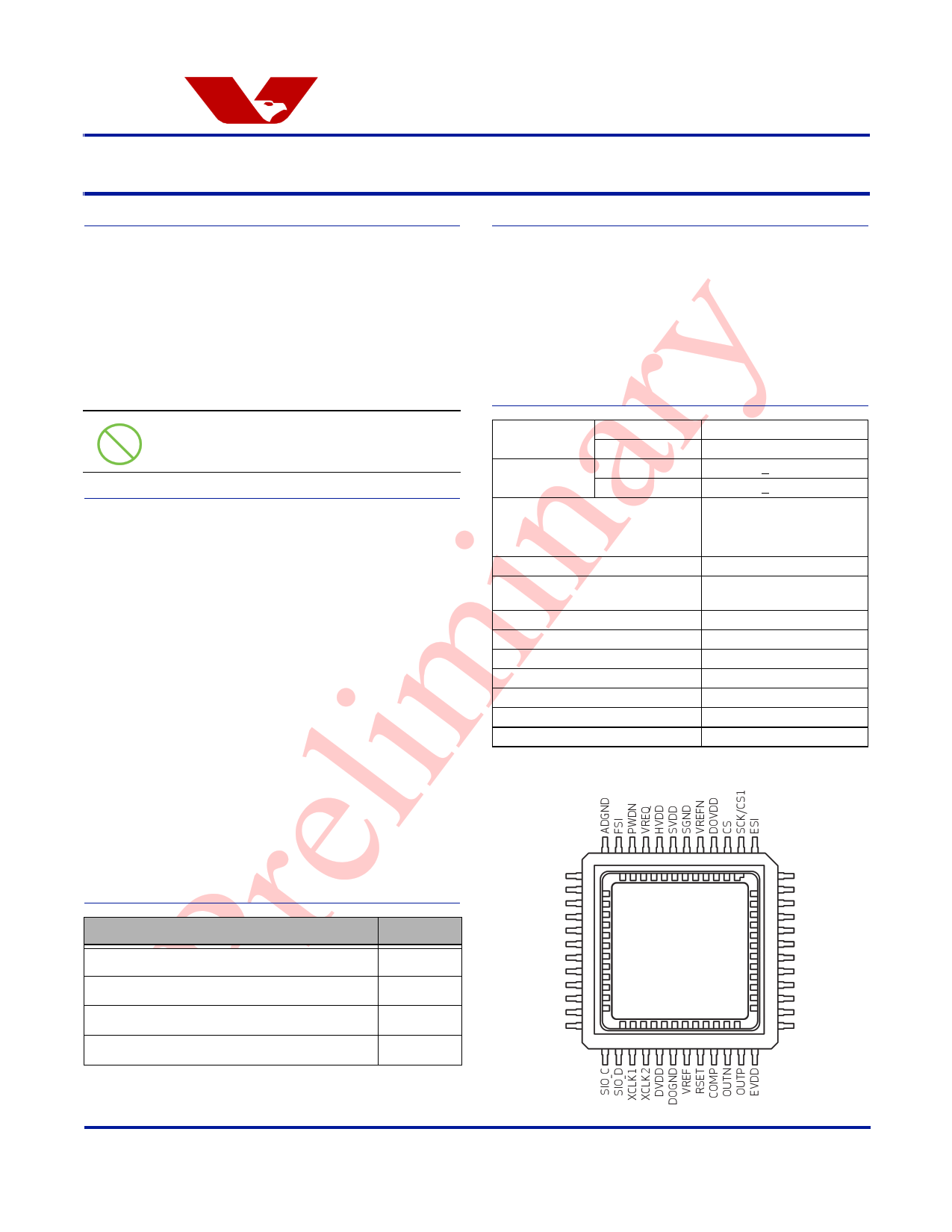
Figure 1 OV7949/OV7449 Pin Diagram (Top View)
ADVDD
NC
NC
NC
NC
NC
NC
NC
NC
NC
NC
FSO/
FSC/CS0
6 5 4 3 2 1 48 47 46 45 44 43
7 42
8 41
9 40
10 39
11 OV7949 / 38
12 37
13 OV7449 36
14 35
15 34
16 33
17 32
18 31
19 20 21 22 23 24 25 26 27 28 29 30
ESO/PAL
NC
NC
NC
NC
NC
NC
NC
NC
NC
NC
EGND
© 2007 OmniVision Technologies, Inc.
Version 1.3, September 29, 2006
7949QFP_DS_001
OmniPixel, OmniVision, and the OmniVision logo are registered trademarks of OmniVision Technologies, Inc.
CameraChip is a trademark of OmniVision Technologies, Inc.
These specifications are subject to change without notice.1
1 page 
Omni ision
Functional Description
Bit Map File
The bit map file starts from address 0x20 where each bit
that equals ’0’ indicates no overlay bit marked and each bit
that equals ’1’ indicates an overlay bit is marked.
Byte[19]
Every time a new line is started, we need to go to a new
address for memory reading. For example, if the user
specifies 500 pixels per line, which is not an exact multiple
of 8, they need at least 63 bytes (63 x 8 = 504) to save the
information. So, they can only specify MemLine[7:0] to be
a number greater than or equal to [3F].
For example, if you want 500 pixels per line and if
MemLine = [40], use hex address [20] to [5E].
Line 1 start address = [20], and the reading sequence as
follows:
Byte[20]bit7, bit6, bit5, bit4, bit3, bit2, bit1, bit0,
Byte[21]bit7, bit6, bit5, bit4, bit3, bit2, bit1, bit0,
Byte[22]bit7, bit6, ....
Byte[5E]bit7, bit6, bit5, bit4 END
Line 2 start address = [60] and it reads through address
[9E], the reading sequence as follows:
Reading sequence:
Byte[60]bit7, bit6, bit5, bit4, bit3, bit2, bit1, bit0,
Byte[61]bit7, bit6, bit5, bit4, bit3, bit2, bit1, bit0,
Byte[62]bit7, bit6, ....
Byte[9E]bit7, bit6, bit5, bit4 END
So, in each line, 500 bits are read.
Multi-Chip Synchronize
The OV7949/OV7449 CAMERACHIP sensor provides the
multi-chip Synchronize function where one chip works as
the master and all others as slave devices. The master
chip provides the frame synchronize signal through pin
FSO. All slave devices then accept the frame synchronize
signal through pin FSI. This mode allows all devices to
synchronize together.
Chip Configuration
The OV7949/OV7449 CAMERACHIP sensor has been
designed for ease-of-use in many stand-alone
applications. Some functions like serial interface slave
address (pins CS0 and CS1) and PAL/NTSC (pin
ESO/PAL) selection can be set by connecting appropriate
pins high (logic "1") or low (logic "0") through a 10 KΩ
resistor. The OV7949/OV7449 CAMERACHIP sensor also
has a serial slave interface for programmable access to all
register functions.
Additional Picture Controls
The OV7949/OV7449 CAMERACHIP sensor provides
additional picture control functions to enhance image
quality and chip performance. These functions are listed
as follows:
• AGC gain range control
• Gamma correction
• Brightness
• Contrast
• Full color bar test pattern
Byte[18:14]
The user can specify the vertical and horizontal
dimensions of the overlay bitmap. If the desired figure is
very small compared to the dimensions of the whole
screen, the user can save a lot of memory.
Byte[13:11]
Y, U, V specifies overlay color.
Byte[10]
When choosing 3x3 or 5x5 resolution, be aware that
because the YUV sampling format is 4:2:2, there may be
strong color aliasing around overlay edge.
Serial Camera Control Bus (SCCB)
Many of the functions and configuration registers in the
OV7949/OV7449 image sensors are available through the
SCCB interface. The OV7949/OV7449 image sensor
operates as a slave device that supports up to 400 kbps
serial transfer rate using a 7-bit address/data transfer
protocol.
SCCB Protocol Format
In SCCB operation (see Figure 6), the master must
perform the following operations:
• Generate the Start/Stop condition
• Provide the serial clock on SIO_C
• Place the 7-bit slave address (RW bit) and the 8-bit
sub-address on SIO_D
Version 1.3, September 29, 2006
Proprietary to OmniVision Technologies, Inc.
5
5 Page 
Omni ision
Timing Specifications
NTSC Timing
Figure 7 NTSC Standard Video Timing Diagram
HSYNC
HSYNC/2
Timing Specifications
HCOUNT/2 HCOUNT/2
analog
field 1
HCOUNT/2 HCOUNT/2
520 521 522 523 524 525
1
2
3
4
5
6
7
analog field 2
start of VSYNC
258 259 260 261 262 263 264 265 266 267 268 269
Figure 8 NTSC Composite Video Signal
13
275 276
7949QFP_DS_007
1.020 V
white level
100 IRE
0.449 V
0.357 V
0.306 V
20 IRE
20 IRE
0.163 V
40 IRE
0.022 V
7.5 IRE
3.58 MHz
color burst
(9 cycles)
black level
blank level
sync level
7949QFP_DS_008
Version 1.3, September 29, 2006
Proprietary to OmniVision Technologies, Inc.
11
11 Page | ||
| Páginas | Total 30 Páginas | |
| PDF Descargar | [ Datasheet OV7449.PDF ] | |
Hoja de datos destacado
| Número de pieza | Descripción | Fabricantes |
| OV7449 | CMOS NTSC/PAL CAMERACHIP Sensor | OmniVision Technologies |
| Número de pieza | Descripción | Fabricantes |
| SLA6805M | High Voltage 3 phase Motor Driver IC. |
Sanken |
| SDC1742 | 12- and 14-Bit Hybrid Synchro / Resolver-to-Digital Converters. |
Analog Devices |
|
DataSheet.es es una pagina web que funciona como un repositorio de manuales o hoja de datos de muchos de los productos más populares, |
| DataSheet.es | 2020 | Privacy Policy | Contacto | Buscar |