|
|
|
PDF XCL202 Data sheet ( Hoja de datos )
| Número de pieza | XCL202 | |
| Descripción | Inductor Built-in Step-Down micro DC/DC Converters | |
| Fabricantes | Torex Semiconductor | |
| Logotipo | ||
Hay una vista previa y un enlace de descarga de XCL202 (archivo pdf) en la parte inferior de esta página. Total 21 Páginas | ||
|
No Preview Available !
XCL201/XCL202 Series
Inductor Built-in Step-Down “micro DC/DC” Converters
ETR2802-003
GreenOperation Compatible
■GENERAL DESCRIPTION
The XCL201/XCL201 series is a synchronous step-down micro DC/DC converter which integrates an inductor and a control IC
in one tiny package (2.5mm×2.0mm, h=1.0mm). A stable power supply with an output current of 400mA is configured using
only two capacitors connected externally.
Operating voltage range is from 2.0V to 6.0V. Output voltage is internally set in a range from 0.8V to 4.0V in increments of
0.05V. The device is operated by 1.2MHz, and includes 0.42ΩP-channel driver transistor and 0.52ΩN-channel switching
transistor. As for operation mode, the XCL201 series is PWM control, the XCL202 series is automatic PWM/PFM switching
control, allowing fast response, low ripple and high efficiency over the full range of loads (from light load to heavy load).
During stand-by, the device is shutdown to reduce current consumption to as low as 1.0μA or less. With the built-in UVLO
(Under Voltage Lock Out) function, the internal driver transistor is forced OFF when input voltage becomes 1.4V or lower. The
series provide short-time turn-on by the soft start function internally set in 0.25ms (TYP). The series integrate CL auto
discharge function which enables the electric charge stored at the output capacitor CL to be discharged via the internal
auto-discharge switch located between the LX and VSS pins. When the devices enter stand-by mode, output voltage quickly
returns to the VSS level as a result of this function.
■APPLICATIONS
Mobile phones, Smart phones
Bluetooth Headsets
WiMAX PDAs, MIDs, UMPCs
Portable game consoles
Digital cameras, Camcorders
SSD(Solid State Drive)
PND(Portable Navigation Device)
■FEATURES
Ultra Small
: 2.5mm 2.0mm, h=1.0mm
Input Voltage
: 2.0V ~ 6.0V
Output Voltage
: 0.8V ~ 4.0V (±2.0%)
High Efficiency
Output Current
: 92%(VIN=4.2V,VOUT=3.3V)
: 400mA
Oscillation Frequency
: 1.2MHz (±15%)
Maximum Duty Cycle
: 100%
Output Capacitor
: Low ESR Ceramic
Current Limiter Circuit
: Constant Current & Latching
Control Methods
: PWM (XCL201)
PWM/PFM Auto (XCL202)
CE Function
: Soft-Start Circuit Built-In
Operating Ambient Temperature : -40 +85
Environmentally Friendly
: EU RoHS Compliant, Pb Free
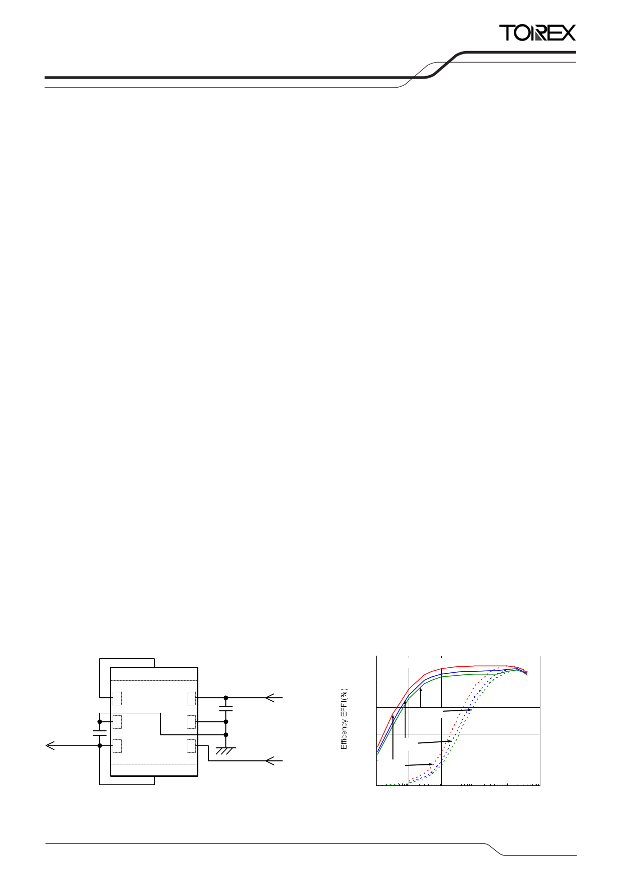
TYPICAL APPLICATION CIRCUIT
XCL201/XCL202 Series
CL
10 F
400mA
L1
LX VIN
Vss Vss
VOUT
L2
CE
CIN
4.7 F
(TOP VIEW)
* “L1 and LX”, and “L2 and VOUT” is connected by wiring.
TYPICAL PERFORMANCE
CHARACTERISTICS
XCL201B331BR/XCL202B331BR
100
XCL202(PWM/PFM)
80
60
VIN= 5.5V
40
5.0V
XCL201(PWM)
20
4.2V
0
0.01
0.1
1
VOUT=3.3V
10 100 1000
Output Current:IOUT (mA)
1/21
1 page 
XCL201/XCL202
Series
■ELECTRICAL CHARACTERISTICS (Continued)
XCL201B181BR/XCL202B181BR, VOUT=1.8V, fOSC=1.2MHz, Ta=25℃
PARAMETER
SYMBOL
CONDITIONS
MIN. TYP. MAX. UNITS CIRCUIT
Output Voltage
Operating Voltage Range
Maximum Output Current
UVLO Voltage
VOUT
VIN
IOUTMAX
VUVLO
When connected to external components,
VIN=VCE=5.0V, IOUT=30mA
VIN=VOUT(E)+2.0V, VCE=1.0V
When connected to external components (*8)
VCE=VIN,VOUT=0V
Voltage which Lx pin holding “L” level (*1, *10)
1.764
2.0
400
1.800 1.836
- 6.0
--
1.00 1.40 1.78
V
V
mA
V
①
①
①
②
Supply Current (XCL201)
Supply Current (XCL202)
IDD VIN=VCE=5.0V, VOUT=VOUT(T) 1.1V
- 22 50 μA ②
- 15 33
Stand-by Current
Oscillation Frequency
ISTB
fOSC
PFM Switching Current (*11)
IPFM
PFM Duty Limit (*11)
Maximum Duty Cycle
Minimum Duty Cycle
DTYLIMIT_PFM
MAXDTY
MINDTY
Efficiency (*2)
EFFI
Lx SW "H" ON Resistance 1
Lx SW "H" ON Resistance 2
Lx SW "L" ON Resistance 1
Lx SW "L" ON Resistance 2
Lx SW "H" Leakage Current (*5)
Current Limit (*9)
Output Voltage
Temperature Characteristics
RL H1
RL H2
RL L1
RL L2
ILeakH
ILIM
VOUT/
(VOUT Topr)
CE "H" Voltage
VCEH
CE "L" Voltage
CE "H" Current
CE "L" Current
Soft Start Time
VCEL
ICEH
ICEL
tSS
Latch Time
tLAT
Short Protection
Threshold Voltage
CL Discharge
Inductance Value
VSHORT
RDCHG
L
VIN=5.0V, VCE=0V, VOUT=VOUT(T) 1.1V
When connected to external components,
VIN=VOUT(T)+2.0V, VCE=1.0V , IOUT=100mA
When connected to external components,
VIN=VOUT(T)+2.0V, VCE=VIN , IOUT=1mA
VCE=VIN=VOUT(T) +0.5V, IOUT=1mA
VIN=VCE=5.0V, VOUT=VOUT (T) 0.9V
VIN=VCE=5.0V, VOUT=VOUT (T) 1.1V
When connected to external components,
VCE=VIN=VOUT (T)+1.2V, IOUT=100mA
VIN=VCE=5.0V, VOUT=0V, ILX=100mA (*3)
VIN=VCE=3.6V, VOUT=0V, ILX=100mA (*3)
VIN=VCE=5.0V (*4)
VIN=VCE=3.6V (*4)
VIN=VOUT=5.0V, VCE=0V, LX=0V
VIN=VCE= 5.0V, VOUT=VOUT (T) 0.9V (*7)
IOUT=30mA
-40 Topr 85
VOUT=0V, Applied voltage to VCE,
Voltage changes Lx to “H” level (*10)
VOUT=0V, Applied
Voltage changes
Lvxolttoag“Le”tolevVeClE(,*10)
VIN=VCE=5.0V, VOUT=0V
VIN=5.0V, VCE=0V, VOUT=0V
When connected to external components,
VCE=0V VIN , IOUT=1mA
VIN=VCE=5.0V, VOUT=0.8 VOUT(T)
Short Lx at 1Ω resistance (*6)
Sweeping VOUT, VIN=VCE=5.0V, Short Lx at
1Ω resistance, VOUT voltage which Lx becomes
“L” level within 1ms
VIN=5.0V LX=5.0V VCE=0V VOUT=open
Test frequency=1MHz
-
1020
0
1200
1.0
1380
μA
kHz
120
-
100
-
-
-
-
-
-
-
700
-
0.65
VSS
- 0.1
- 0.1
-
1.0
160
200
-
-
89
0.35
0.42
0.45
0.52
0.01
800
100
200 mA
300 %
-%
0%
-%
0.55
0.67
0.66
0.77
1.0
1000
Ω
Ω
Ω
Ω
A
mA
- ppm/
- 6.0 V
- 0.25 V
- 0.1 μA
- 0.1 μA
0.32 0.50 ms
- 20 ms
0.675 0.900 1.125 V
200 300 450
Ω
- 4.7 - μH
③
①
⑩
①
③
③
①
④
④
-
-
⑨
⑥
①
③
③
⑤
⑤
①
⑦
⑦
⑧
-
Allowed Inductor Current
IDC
T=40
- 600 - mA -
Test conditions: Unless otherwise stated, VIN=5.0V, VOUT (T)=Nominal Voltage
NOTE:
(*1) Including hysteresis operating voltage range.
(*2) EFFI={ ( output voltage×output current ) / ( input voltage×input current) }×100
(*3)
(*4)
ON resistance
Design value
(Ω)=(VIN
-
Lx
pin
measurement
voltage)
/
100mA
(*5) When temperature is high, a current of approximately 10μA (maximum) may leak.
(*6)
(*7)
(*8)
Time until
When VIN
When the
it short-circuits VOUT with GND via 1Ω of resistor from an operational state and is set to Lx=0V from current limit pulse generating.
is less than 2.4V, limit current may not be reached because voltage falls caused by ON resistance.
difference between the input and the output is small, some cycles may be skipped completely before current maximizes.
If current is further pulled from this state, output voltage will decrease because of P-ch driver ON resistance.
(*9) Current limit denotes the level of detection at peak of coil current.
(*10) “H”=VIN~VIN-1.2V, “L”=+0.1V~-0.1V
(*11) IPFM and DTYLIMIT_PFM are defined only for the XCL202 series which have PFM control function. (Not for the XCL201 series)
5/21
5 Page 
XCL201/XCL202
Series
■NOTE ON USE
1. The XCL201/XCL202 series is designed for use with ceramic output capacitors. If, however, the potential difference is too large between
the input voltage and the output voltage, a ceramic capacitor may fail to absorb the resulting high switching energy and oscillation could
occur on the output. If the input-output potential difference is large, connect an electrolytic capacitor in parallel to compensate for
insufficient capacitance.
2. Spike noise and ripple voltage arise in a switching regulator as with a DC/DC converter. These are greatly influenced by external
component selection, such as the coil inductance, capacitance values, and board layout of external components. Once the design has been
completed, verification with actual components should be done.
3. Depending on the input-output voltage differential, or load current, some pulses may be skipped, and the ripple voltage may increase.
4. When the difference between input and output is large in PWM control, very narrow pulses will be outputted, and there is the possibility that
some cycles may be skipped completely.
5. When the difference between input and output is small, and the load current is heavy, very wide pulses will be outputted and there is the
possibility that some cycles may be skipped completely.
6. With the IC, the peak current of the coil is controlled by the current limit circuit. Since the peak current increases when dropout voltage or
load current is high, current limit starts operation, and this can lead to instability. When peak current becomes high, please adjust the coil
inductance value and fully check the circuit operation. In addition, please calculate the peak current according to the following formula:
Ipk = (VIN - VOUT) x OnDuty / (2 x L x fOSC) + IOUT
L: Coil Inductance Value
fOSC: Oscillation Frequency
7. When the peak current which exceeds limit current flows within the specified time, the built-in P-ch driver transistor turns off. During the
time until it detects limit current and before the built-in transistor can be turned off, the current for limit current flows; therefore, care must be
taken when selecting the rating for the external components such as a coil.
8. When VIN is less than 2.4V, limit current may not be reached because voltage falls caused by ON resistance.
9. Depending on the state of the PC Board, latch time may become longer and latch operation may not work. In order to avoid the effect of
noise, the board should be laid out so that input capacitors are placed as close to the IC as possible.
10. Use of the IC at voltages below the recommended voltage range may lead to instability.
11. This IC should be used within the stated absolute maximum ratings in order to prevent damage to the device.
12. When the IC is used in high temperature, output voltage may increase up to input voltage level at no load because of the leak current of
the driver transistor.
13. The current limit is set to 1000mA (MAX.) at typical. However, the current of 1000mA or more may flow.
In case that the current limit functions while the VOUT pin is shorted to the GND pin, when P-ch MOSFET is ON, the potential difference for
input voltage will occur at both ends of a coil. For this, the time rate of coil current becomes large. By contrast, when N-ch MOSFET is
ON, there is almost no potential difference at both ends of the coil since the VOUT pin is shorted to the GND pin. Consequently, the time
rate of coil current becomes quite small. According to the repetition of this operation, and the delay time of the circuit, coil current will be
converged on a certain current value, exceeding the amount of current, which is supposed to be limited originally. Even in this case,
however, after the over current state continues for several ms, the circuit will be latched. A coil should be used within the stated absolute
maximum rating in order to prevent damage to the device.
①Current flows into P-ch MOSFET to reach the current limit (ILIM).
②The current of ILIM or more flows since the delay time of the circuit occurs during from the detection of the current limit to OFF of P-ch MOSFET.
③Because of no potential difference at both ends of the coil, the time rate of coil current becomes quite small.
④Lx oscillates very narrow pulses by the current limit for several ms.
⑤The circuit is latched, stopping its operation.
②
①③
Duty
④
Limit > #ms
⑤
Lx
ILIM
ILx
11/21
11 Page | ||
| Páginas | Total 21 Páginas | |
| PDF Descargar | [ Datasheet XCL202.PDF ] | |
Hoja de datos destacado
| Número de pieza | Descripción | Fabricantes |
| XCL201 | Inductor Built-in Step-Down micro DC/DC Converters | Torex Semiconductor |
| XCL202 | Inductor Built-in Step-Down micro DC/DC Converters | Torex Semiconductor |
| XCL205 | Inductor Built-in Step-Down micro DC/DC Converters | Torex Semiconductor |
| XCL206 | Inductor Built-in Step-Down micro DC/DC Converters | Torex Semiconductor |
| Número de pieza | Descripción | Fabricantes |
| SLA6805M | High Voltage 3 phase Motor Driver IC. |
Sanken |
| SDC1742 | 12- and 14-Bit Hybrid Synchro / Resolver-to-Digital Converters. |
Analog Devices |
|
DataSheet.es es una pagina web que funciona como un repositorio de manuales o hoja de datos de muchos de los productos más populares, |
| DataSheet.es | 2020 | Privacy Policy | Contacto | Buscar |