|
|
|
PDF FDS6986AS Data sheet ( Hoja de datos )
| Número de pieza | FDS6986AS | |
| Descripción | Dual Notebook Power Supply N-Channel PowerTrench SyncFET | |
| Fabricantes | Fairchild Semiconductor | |
| Logotipo | ||
Hay una vista previa y un enlace de descarga de FDS6986AS (archivo pdf) en la parte inferior de esta página. Total 10 Páginas | ||
|
No Preview Available !
March 2005
FDS6986AS
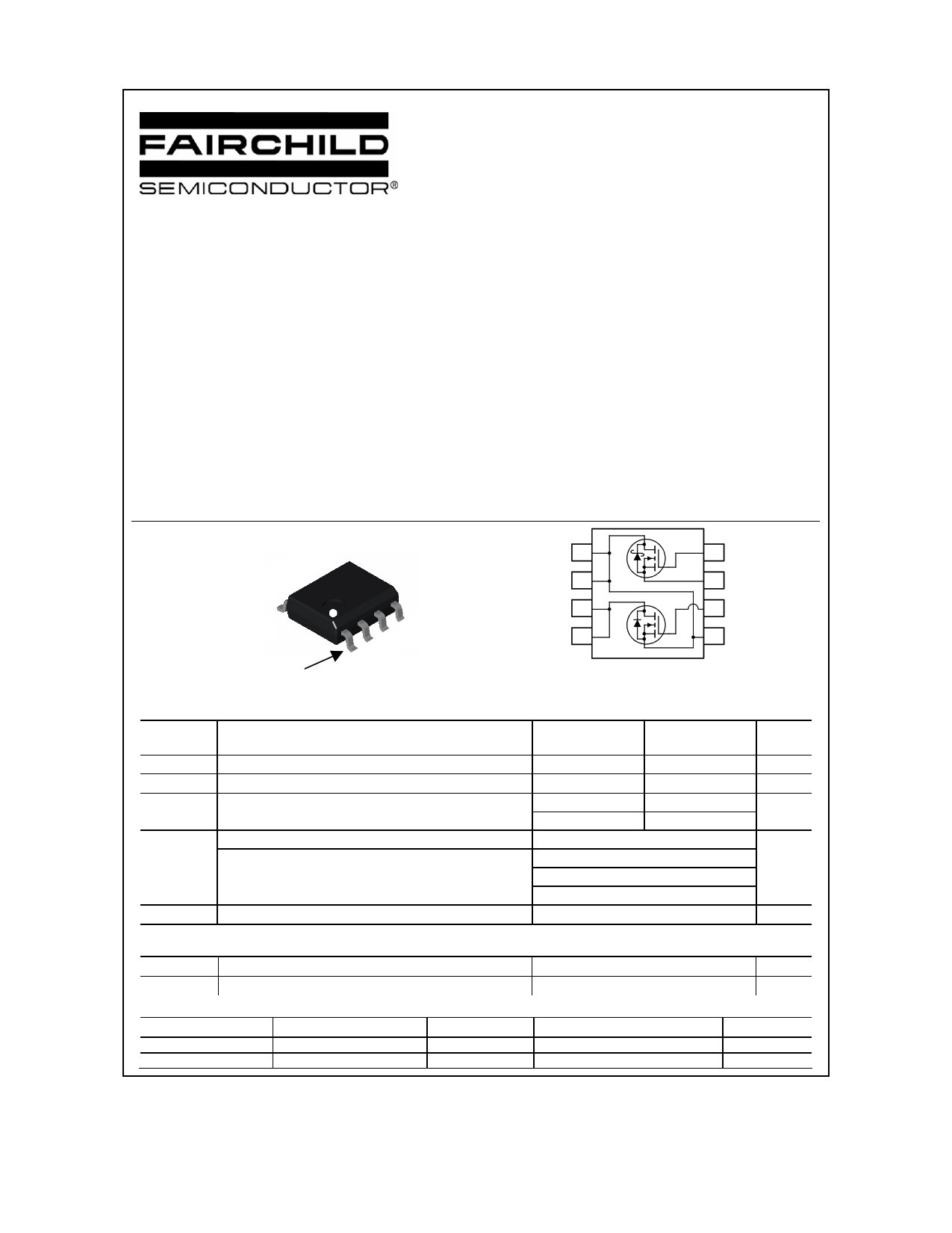
Dual Notebook Power Supply N-Channel PowerTrench® SyncFET™
General Description
Features
The FDS6986AS is designed to replace two single SO-
8 MOSFETs and Schottky diode in synchronous
DC:DC power supplies that provide various peripheral
voltages for notebook computers and other battery
powered electronic devices. FDS6986AS contains two
unique 30V, N-channel, logic level, PowerTrench
MOSFETs designed to maximize power conversion
efficiency.
The high-side switch (Q1) is designed with specific
emphasis on reducing switching losses while the low-
side switch (Q2) is optimized to reduce conduction
losses. Q2 also includes an integrated Schottky diode
using Fairchild’s monolithic SyncFET technology.
• Q2: Optimized to minimize conduction losses
Includes SyncFET Schottky body diode
7.9A, 30V
RDS(on) = 20 mΩ @ VGS = 10V
RDS(on) = 28 mΩ @ VGS = 4.5V
• Q1: Optimized for low switching losses
Low gate charge (10 nC typical)
6.5A, 30V
RDS(on) = 29 mΩ @ VGS = 10V
RDS(on) = 38 mΩ @ VGS = 4.5V
D
D
D
D
SO-8
Pin 1 SO-8
G
SS
S
Absolute Maximum Ratings TA = 25°C unless otherwise noted
Symbol
VDSS
VGSS
ID
PD
TJ, TSTG
Parameter
Drain-Source Voltage
Gate-Source Voltage
Drain Current - Continuous
- Pulsed
Power Dissipation for Dual Operation
(Note 1a)
Power Dissipation for Single Operation
(Note 1a)
(Note 1b)
(Note 1c)
Operating and Storage Junction Temperature Range
Thermal Characteristics
RθJA Thermal Resistance, Junction-to-Ambient (Note 1a)
RθJC
Thermal Resistance, Junction-to-Case
(Note 1)
Package Marking and Ordering Information
Device Marking
Device
Reel Size
FDS6986AS
FDS6986AS
FDS6986AS
FDS6986AS_NL (Note 4)
13”
13”
©2005 Fairchild Semiconductor Corporation
Q2
5
6
7 Q1
8
4
3
2
1
Q2 Q1
30 30
±20 ±16
7.9 6.5
30 20
2
1.6
1
0.9
–55 to +150
Units
V
V
A
W
°C
78
40
Tape width
12mm
12mm
°C/W
°C/W
Quantity
2500 units
2500 units
FDS6986AS Rev A(X)
1 page 
Typical Characteristics: Q2
10
ID = 7.9A
8
6
VDS = 10V
20V
15V
4
2
0
0 3 6 9 12
Qg, GATE CHARGE (nC)
Figure 7. Gate Charge Characteristics.
100
10 RDS(ON) LIMIT
1
100µs
1ms
10ms
100ms
1s
10s
DC
VGS = 10V
0.1 SINGLE PULSE
RθJA = 135oC/W
TA = 25oC
0.01
0.01
0.1 1 10
VDS, DRAIN-SOURCE VOLTAGE (V)
100
Figure 9. Maximum Safe Operating Area.
800
f = 1MHz
VGS = 0 V
600
Ciss
400
Coss
200
Crss
0
0
4 8 12 16
VDS, DRAIN TO SOURCE VOLTAGE (V)
20
Figure 8. Capacitance Characteristics.
50
SINGLE PULSE
RθJA = 135°C/W
40 TA = 25°C
30
20
10
0
0.001
0.01
0.1 1
t1, TIME (sec)
10
Figure 10. Single Pulse Maximum
Power Dissipation.
100
FDS6986AS Rev A (X)
5 Page | ||
| Páginas | Total 10 Páginas | |
| PDF Descargar | [ Datasheet FDS6986AS.PDF ] | |
Hoja de datos destacado
| Número de pieza | Descripción | Fabricantes |
| FDS6986AS | Dual Notebook Power Supply N-Channel PowerTrench SyncFET | Fairchild Semiconductor |
| Número de pieza | Descripción | Fabricantes |
| SLA6805M | High Voltage 3 phase Motor Driver IC. |
Sanken |
| SDC1742 | 12- and 14-Bit Hybrid Synchro / Resolver-to-Digital Converters. |
Analog Devices |
|
DataSheet.es es una pagina web que funciona como un repositorio de manuales o hoja de datos de muchos de los productos más populares, |
| DataSheet.es | 2020 | Privacy Policy | Contacto | Buscar |