|
|
|
PDF STMP3630XXBBEB1M Data sheet ( Hoja de datos )
| Número de pieza | STMP3630XXBBEB1M | |
| Descripción | Audio System on Chip | |
| Fabricantes | Sigmatel | |
| Logotipo | ||
Hay una vista previa y un enlace de descarga de STMP3630XXBBEB1M (archivo pdf) en la parte inferior de esta página. Total 30 Páginas | ||
|
No Preview Available !
PRODUCT DATA SHEET
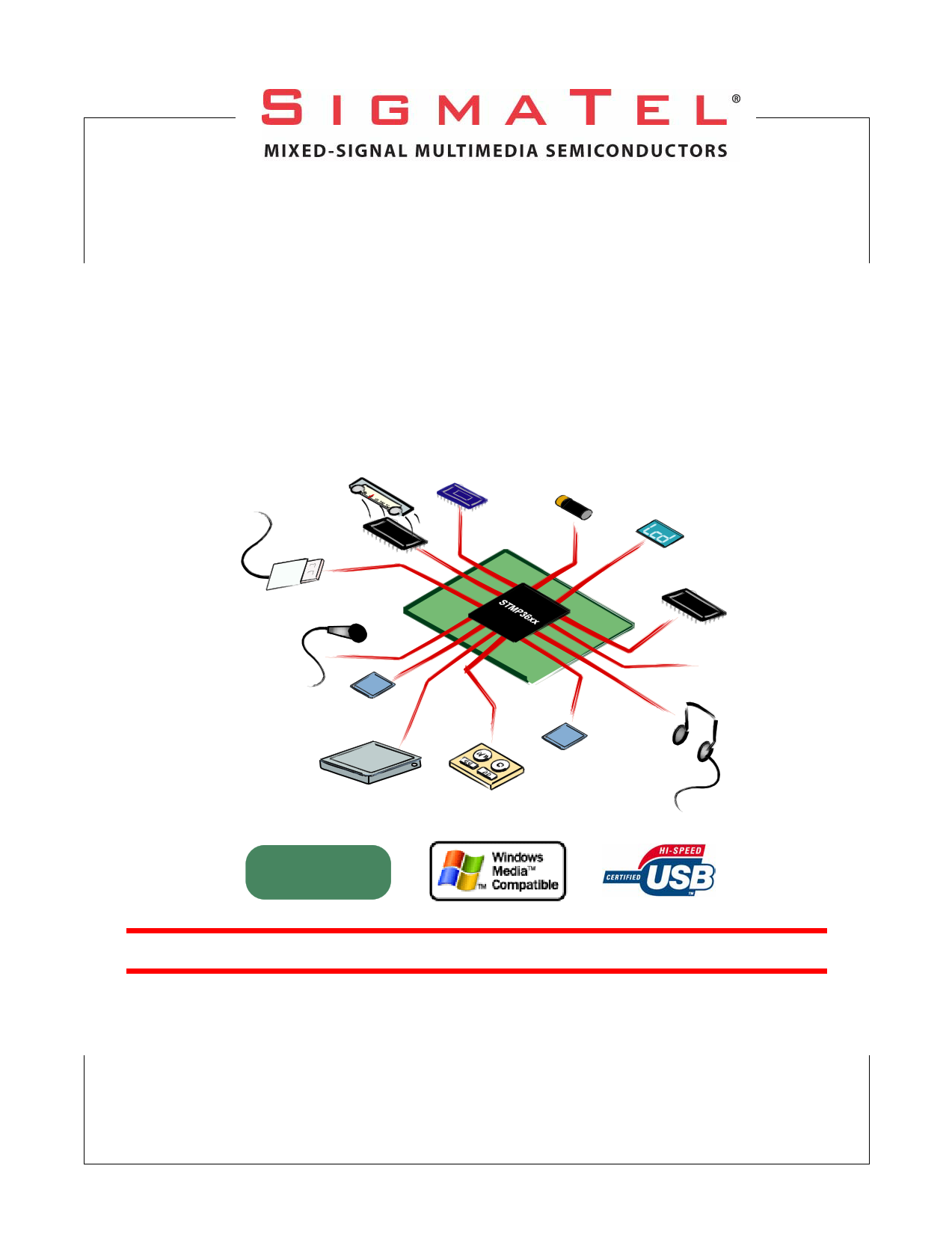
STMP36xx
Audio System on Chip
with USB OTG, LCD, Hard Drive, and Battery Charger
Fourth-Generation Audio Decoder
Version 1.02 May 3, 2006
FM Tuner
Host Processor (Optional)
Rechargeable
Battery
LED/LCD/Color
Display
Hi-Speed USB
On-the-Go
Microphone
Voice Record
NAND Flash
SDRAM/NOR
SPDIF
Hard Drive
SD/SDIO/MS
Buttons/Switches
Headphones
ISO9001:2000 Certified
IEC QC 080000:2005
(IECQ HSPM) Certified
OFFICIAL PRODUCT DOCUMENTATION 5/3/06
5-36xx-D1-1.02-050306
Copyright © 2003-2006 SigmaTel, Inc.
All rights reserved.
SigmaTel, Inc. makes no warranty for the use of its products, assumes no responsibility for any errors which may appear in this document, and makes
no commitment to update the information contained herein. SigmaTel reserves the right to change or discontinue this product at any time, without no-
tice. There are no express or implied licenses granted hereunder to design or fabricate any integrated circuits based on information in this document.
The following are trademarks of SigmaTel, Inc., and may be used to identify SigmaTel products only: SigmaTel, the SigmaTel Logo, C Major, D Major
and Go-Chip. Windows Media and the Windows logo are trademarks or registered trademarks of Microsoft Corporation in the United States and/or
other countries. Other product and company names contained herein may be trademarks of their respective owners.
Free Datasheet http://www.datasheet4u.com/
1 page 
OFFICIAL PRODUCT DOCUMENTATION 5/3/06
STMP36xx
7. DIGITAL CONTROL AND ON-CHIP RAM ................................................................................. 123
7.1. Overview ....................................................................................................................................... 123
7.2. SRAM Controls ............................................................................................................................. 124
7.2.1. SRAM BIST Control ........................................................................................................ 126
7.3. ROM Controls ............................................................................................................................... 127
7.4. Miscellaneous Controls ................................................................................................................. 127
7.4.1. Performance Monitoring .................................................................................................. 127
7.4.2. High-Entropy PRN Seed ................................................................................................. 127
7.4.3. Write-Once Register ........................................................................................................ 128
7.4.4. Microseconds Counter .................................................................................................... 128
7.5. Behavior During Reset .................................................................................................................. 128
7.6. Programmable Registers .............................................................................................................. 128
7.6.1. DIGCTL Control Register Description ............................................................................. 128
7.6.2. DIGCTL Status Register Description .............................................................................. 130
7.6.3. Free-Running HCLK Counter Register Description ......................................................... 131
7.6.4. On-Chip RAM Control Register Description .................................................................... 131
7.6.5. On-Chip RAM Repair Data 0 Register Description ......................................................... 133
7.6.6. On-Chip RAM Repair Data 1 Register Description ......................................................... 134
7.6.7. Software Write-Once Register Description ...................................................................... 135
7.6.8. AHB Transfer Count Register Description ...................................................................... 136
7.6.9. AHB Performance Metric for Stalled Bus Cycles Register Description ........................... 136
7.6.10. Entropy Register Description ........................................................................................ 137
7.6.11. Digital Control ROM Shield Read Enable Register Description .................................... 138
7.6.12. Digital Control Microseconds Counter Register Description ......................................... 138
7.6.13. Digital Control Debug Read Test Register Description ................................................. 139
7.6.14. Digital Control Debug Register Description ................................................................... 139
7.6.15. SRAM BIST Control and Status Register Description ................................................... 140
7.6.16. SRAM BIST Repair Register 0 Description ................................................................... 140
7.6.17. SRAM BIST Repair Register 1 Description ................................................................... 141
7.6.18. SRAM Status Register 0 Description ............................................................................ 142
7.6.19. SRAM Status Register 1 Description ............................................................................ 142
7.6.20. SRAM Status Register 2 Description ............................................................................ 143
7.6.21. SRAM Status Register 3 Description ............................................................................ 143
7.6.22. SRAM Status Register 4 Description ............................................................................ 144
7.6.23. SRAM Status Register 5 Description ............................................................................ 144
7.6.24. SRAM Status Register 6 Description ............................................................................ 145
7.6.25. SRAM Status Register 7 Description ............................................................................ 145
7.6.26. SRAM Status Register 8 Description ............................................................................ 146
7.6.27. SRAM Status Register 9 Description ............................................................................ 146
7.6.28. SRAM Status Register 10 Description .......................................................................... 147
7.6.29. SRAM Status Register 11 Description .......................................................................... 147
7.6.30. SRAM Status Register 12 Description .......................................................................... 148
7.6.31. SRAM Status Register 13 Description .......................................................................... 149
7.6.32. Digital Control Scratch Register 0 Description .............................................................. 150
7.6.33. Digital Control Scratch Register 1 Description .............................................................. 150
7.6.34. Digital Control ARM Cache Register Description .......................................................... 151
7.6.35. SigmaTel Copyright Identifier Register Description ....................................................... 151
7.6.36. Digital Control Chip Revision Register Description ....................................................... 152
8. USB HIGH-SPEED ON-THE-GO (HOST/DEVICE) CONTROLLER .......................................... 155
8.1. Overview ....................................................................................................................................... 155
8.2. USB Controller Core ..................................................................................................................... 155
8.3. USB Programmed I/O (PIO) Target Interface ............................................................................... 157
8.4. USB DMA Interface ....................................................................................................................... 157
8.5. USB UTMI Interface ...................................................................................................................... 157
8.5.1. Exporting the PHY ........................................................................................................... 157
8.5.2. Digital/Analog Loopback Test Mode ............................................................................... 157
8.6. USB Controller Flowcharts ............................................................................................................ 158
9. INTEGRATED USB 2.0 PHY ...................................................................................................... 161
9.1. Overview ....................................................................................................................................... 161
9.2. External Signals ............................................................................................................................ 161
9.3. UTMI and Digital Circuits .............................................................................................................. 162
5-36xx-D1-1.02-050306
Contents
5
Free Datasheet http://www.datasheet4u.com/
5 Page 
OFFICIAL PRODUCT DOCUMENTATION 5/3/06
STMP36xx
17.6.20. PINCTRL Bank 1 Interrupt Mask Register Description ............................................... 453
17.6.21. PINCTRL Bank 1 Interrupt Level/Edge Register Description ...................................... 454
17.6.22. PINCTRL Bank 1 Interrupt Polarity Register Description ............................................ 455
17.6.23. PINCTRL Bank 1 Interrupt Status Register Description .............................................. 456
17.6.24. PINCTRL Bank 2 Lower Pin Mux Select Register Description .................................... 456
17.6.25. PINCTRL Bank 2 Upper Pin Mux Select Register Description .................................... 457
17.6.26. PINCTRL Bank 2 Drive Strength Register Description ............................................... 458
17.6.27. PINCTRL Bank 2 Data Output Register Description ................................................... 459
17.6.28. PINCTRL Bank 2 Data Input Register Description ...................................................... 459
17.6.29. PINCTRL Bank 2 Output Enable Register Description ............................................... 460
17.6.30. PINCTRL Bank 2 Interrupt Select Register Description .............................................. 461
17.6.31. PINCTRL Bank 2 Interrupt Mask Register Description ............................................... 461
17.6.32. PINCTRL Bank 2 Interrupt Level/Edge Register Description ...................................... 462
17.6.33. PINCTRL Bank 2 Interrupt Polarity Register Description ............................................ 463
17.6.34. PINCTRL Bank 2 Interrupt Status Register Description .............................................. 463
17.6.35. PINCTRL Bank 3 Lower Pin Mux Select Register Description .................................... 464
17.6.36. PINCTRL Bank 3 Upper Pin Mux Select Register Description .................................... 465
17.6.37. PINCTRL Bank 3 Drive Strength Register Description ............................................... 466
17.6.38. PINCTRL Bank 3 Data Output Register Description ................................................... 467
17.6.39. PINCTRL Bank 3 Data Input Register Description ...................................................... 468
17.6.40. PINCTRL Bank 3 Output Enable Register Description ............................................... 469
17.6.41. PINCTRL Bank 3 Interrupt Select Register Description .............................................. 469
17.6.42. PINCTRL Bank 3 Interrupt Mask Register Description ............................................... 470
17.6.43. PINCTRL Bank 3 Interrupt Level/Edge Register Description ...................................... 471
17.6.44. PINCTRL Bank 3 Interrupt Polarity Register Description ............................................ 472
17.6.45. PINCTRL Bank 3 Interrupt Status Register Description .............................................. 473
18. TIMERS AND ROTARY DECODER ........................................................................................... 475
18.1. Overview ..................................................................................................................................... 475
18.2. Timers ......................................................................................................................................... 476
18.2.1. Using External Signals as Inputs .................................................................................. 477
18.2.2. Timer 3 and Duty Cycle Mode ....................................................................................... 478
18.2.3. Testing Timer 3 Duty Cycle Modes ............................................................................... 479
18.3. Rotary Decoder ........................................................................................................................... 480
18.3.1. Testing the Rotary Decoder .......................................................................................... 482
18.3.2. Behavior During Reset .................................................................................................. 482
18.4. Programmable Registers ............................................................................................................ 483
18.4.1. Rotary Decoder Control Register Description ............................................................... 483
18.4.2. Rotary Decoder Up/Down Counter Register Description .............................................. 484
18.4.3. Timer 0 Control and Status Register Description .......................................................... 485
18.4.4. Timer 0 Count Register Description .............................................................................. 487
18.4.5. Timer 1 Control and Status Register Description .......................................................... 487
18.4.6. Timer 1 Count Register Description .............................................................................. 489
18.4.7. Timer 2 Control and Status Register Description .......................................................... 490
18.4.8. Timer 2 Count Register Description .............................................................................. 491
18.4.9. Timer 3 Control and Status Register Description .......................................................... 492
18.4.10. Timer 3 Count Register Description ............................................................................ 494
19. REAL-TIME CLOCK, ALARM, WATCHDOG, AND PERSISTENT BITS .................................. 497
19.1. Overview ..................................................................................................................................... 497
19.2. Real-Time Clock ......................................................................................................................... 502
19.2.1. Behavior During Reset .................................................................................................. 502
19.3. Millisecond Resolution Timing Facility ........................................................................................ 502
19.4. Alarm Clock ................................................................................................................................. 502
19.5. Watchdog Reset Register ........................................................................................................... 503
19.6. Laser Fuse Bits ........................................................................................................................... 503
19.7. Programmable Registers ............................................................................................................ 503
19.7.1. Real-Time Clock Control Register Description .............................................................. 503
19.7.2. Real-Time Clock Status Register Description ............................................................... 505
19.7.3. Real-Time Clock Milliseconds Counter Description ...................................................... 506
19.7.4. Real-Time Clock Seconds Counter Register Description .............................................. 507
19.7.5. Real-Time Clock Alarm Register Description ................................................................ 508
19.7.6. Watchdog Timer Register Description .......................................................................... 508
5-36xx-D1-1.02-050306
Contents
11
Free Datasheet http://www.datasheet4u.com/
11 Page | ||
| Páginas | Total 30 Páginas | |
| PDF Descargar | [ Datasheet STMP3630XXBBEB1M.PDF ] | |
Hoja de datos destacado
| Número de pieza | Descripción | Fabricantes |
| STMP3630XXBBEB1M | Audio System on Chip | Sigmatel |
| STMP3630XXBBEB1N | Audio System on Chip | Sigmatel |
| Número de pieza | Descripción | Fabricantes |
| SLA6805M | High Voltage 3 phase Motor Driver IC. |
Sanken |
| SDC1742 | 12- and 14-Bit Hybrid Synchro / Resolver-to-Digital Converters. |
Analog Devices |
|
DataSheet.es es una pagina web que funciona como un repositorio de manuales o hoja de datos de muchos de los productos más populares, |
| DataSheet.es | 2020 | Privacy Policy | Contacto | Buscar |