|
|
|
PDF NB6L14S Data sheet ( Hoja de datos )
| Número de pieza | NB6L14S | |
| Descripción | 2.5V 1:4 AnyLevel Differential Input to LVDS Fanout Buffer/Translator | |
| Fabricantes | ON Semiconductor | |
| Logotipo | ||
Hay una vista previa y un enlace de descarga de NB6L14S (archivo pdf) en la parte inferior de esta página. Total 11 Páginas | ||
|
No Preview Available !
NB6L14S
2.5 V 1:4 AnyLevel]
Differential Input to LVDS
Fanout Buffer/Translator
The NB6L14S is a differential 1:4 Clock or Data Receiver and will
accept AnyLevel differential input signals: LVPECL, CML, LVDS, or
HSCL. These signals will be translated to LVDS and four identical
copies of Clock or Data will be distributed, operating up to 2.0 GHz or
2.5 Gb/s, respectively. As such, the NB6L14S is ideal for SONET,
GigE, Fiber Channel, Backplane and other Clock or Data distribution
applications.
The NB6L14S has a wide input common mode range from
GND + 50 mV to VCC − 50 mV. Combined with the 50 W internal
termination resistors at the inputs, the NB6L14S is ideal for translating
a variety of differential or single−ended Clock or Data signals to
350 mV typical LVDS output levels.
The NB6L14S is the 2.5 V version of the NB6N14S and is offered in
a small 3 mm x 3 mm 16−QFN package. Application notes, models,
and support documentation are available at www.onsemi.com.
The NB6L14S is a member of the ECLinPS MAX™ family of high
performance products.
Features
• Maximum Input Clock Frequency > 2.0 GHz
• Maximum Input Data Rate > 2.5 Gb/s
• 1 ps Maximum of RMS Clock Jitter
• Typically 10 ps of Data Dependent Jitter
• 380 ps Typical Propagation Delay
• 120 ps Typical Rise and Fall Times
• Single Power Supply; VCC = 2.5 $ 5%
• VREF_AC Reference Output
• These are Pb−Free Devices
Device DDJ = 10 ps
http://onsemi.com
1
QFN−16
MN SUFFIX
CASE 485G
MARKING
DIAGRAM*
16
1
NB6L
14S
ALYW G
G
A = Assembly Location
L = Wafer Lot
Y = Year
W = Work Week
G = Pb−Free Package
(Note: Microdot may be in either location)
*For additional marking information, refer to
Application Note AND8002/D.
Q0
Q0
IN
VT
IN
50 W
50 W
EN
(LVTTL/CMOS)
VREFAC
DQ
Q1
Q1
Q2
Q2
Q3
Q3
Figure 1. Logic Diagram
ORDERING INFORMATION
See detailed ordering and shipping information in the package
dimensions section on page 10 of this data sheet.
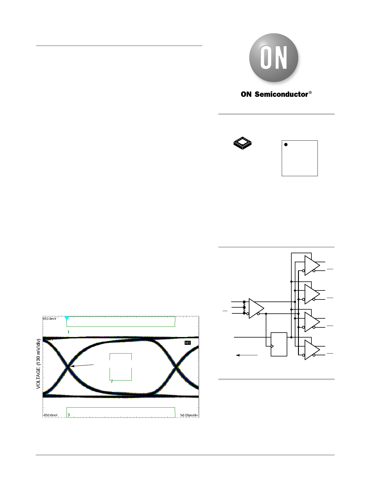
TIME (58 ps/div)
Figure 2. Typical Output Waveform at 2.488 Gb/s with
PRBS 223−1 (VINPP = 400 mV; Input Signal DDJ = 14 ps)
© Semiconductor Components Industries, LLC, 2011
October, 2011 − Rev. 2
1
Publication Order Number:
NB6L14S/D
1 page 
NB6L14S
Table 6. AC CHARACTERISTICS VCC = 2.375 V to 2.625 V, GND = 0 V; (Note 12)
Symbol
finMax
VOUTPP
Characteristic
Maximum Input Clock Frequency
Output Voltage
(Figure 4)
Amplitude
(@
VINPPmin)
fDATA
tPLH,
tPHL
ts
th
tSKEW
Maximum Operating Data Rate
Differential Input to Differential Output, IN to Q
Propagation Delay @ 100 MHz
Setup Time
Hold Time
Within Device Skew (Note 17)
Device−to−Device Skew (Note 16)
ffinin=≤
1.0
1.5
GHz
GHz
fin= 2.0 GHz
EN to IN/IN
−40°C to +85°C
Min Typ Max
2.0
220 350
200 300
170 270
2.5
300 450 600
300 20
500 20
5 20
30 200
Unit
GHz
mV
Gb/s
ps
ps
tJITTER
VINPP
RMS Random Clock Jitter (Note 14)
Deterministic Jitter (Note 15)
Input Voltage Swing/Sensitivity
(Differential Configuration) (Note 13)
fDATA
vfin2=.428.80
GHz
Gb/s
0.5 0.8 ps
5.0 20
100 VCC−GND mV
tr Output Rise/Fall Times @ 250 MHz
tf (20% − 80%)
Q, Q
70 150 225 ps
NOTE: Device will meet the specifications after thermal equilibrium has been established when mounted in a test socket or printed circuit
board with maintained transverse airflow greater than 500 lfpm. Electrical parameters are guaranteed only over the declared
operating temperature range. Functional operation of the device exceeding these conditions is not implied. Device specification limit
values are applied individually under normal operating conditions and not valid simultaneously.
12. Measured by forcing VINPPmin with 50% duty cycle clock source and VCC − 1400 mV offset. All loading with an external RL = 100 W. Input
edge rates 150 ps (20%−80%). See Figure 20.
13. Input voltage swing is a single−ended measurement operating in differential mode.
14. RMS jitter with 50% Duty Cycle clock signal at 750 MHz.
15. Deterministic jitter with input NRZ data at PRBS 223−1 and K28.5.
16. Skew is measured between outputs under identical transition @ 250 MHz.
17. The worst case condition between Q0/Q0 and Q1/Q1 from either D0/D0 or D1/D1, when both outputs have the same transition.
400
350
300
250
200
150
100
50
0
0 0.5 1 1.5 2 2.5 3
INPUT CLOCK FREQUENCY (GHz)
Figure 4. Output Voltage Amplitude (VOUTPP) versus
Input Clock Frequency (fin) and Temperature (@ VCC = 2.5 V)
http://onsemi.com
5
5 Page 
NB6L14S
PACKAGE DIMENSIONS
QFN16 3x3, 0.5P
CASE 485G−01
ISSUE E
D
PIN 1
ÇÇÇÇÇÇÇÇÇLOCATION
A
B
E
LL
L1
DETAIL A
ALTERNATE TERMINAL
CONSTRUCTIONS
NOTES:
1. DIMENSIONING AND TOLERANCING PER
ASME Y14.5M, 1994.
2. CONTROLLING DIMENSION: MILLIMETERS.
3. DIMENSION b APPLIES TO PLATED
TERMINAL AND IS MEASURED BETWEEN
0.25 AND 0.30 MM FROM TERMINAL.
4. COPLANARITY APPLIES TO THE EXPOSED
PAD AS WELL AS THE TERMINALS.
MILLIMETERS
DIM MIN MAX
2X 0.10 C
2X 0.10 C TOP VIEW
0.05 C
DETAIL B
(A3)
A3
ÉÉÉÉ ÉÇÉÇEXPOSED Cu
MOLD CMPD
A1
DETAIL B
A 0.80 1.00
A1 0.00 0.05
A3 0.20 REF
b 0.18 0.30
D 3.00 BSC
D2 1.65 1.85
E 3.00 BSC
E2 1.65 1.85
e 0.50 BSC
0.05 C
A ALTERNATE
CONSTRUCTIONS
K 0.18 TYP
L 0.30 0.50
NOTE 4
L1 0.00 0.15
SIDE VIEW
16X L DETAIL A
D2
8
A1
C
SEATING
PLANE
0.10 C A B
RECOMMENDED
SOLDERING FOOTPRINT*
16X
0.58
PACKAGE
OUTLINE
16X K
49
E2
1
16
e
16X b
0.10
e/2
BOTTOM VIEW
0.05
CAB
C NOTE 3
1
2X 2X
1.84 3.30
16X
0.30
0.50
PITCH
DIMENSIONS: MILLIMETERS
*For additional information on our Pb−Free strategy and soldering
details, please download the ON Semiconductor Soldering and
Mounting Techniques Reference Manual, SOLDERRM/D.
AnyLevel and ECLinPS MAX are trademarks of Semiconductor Components Industries, LLC (SCILLC).
ON Semiconductor and
are registered trademarks of Semiconductor Components Industries, LLC (SCILLC). SCILLC reserves the right to make changes without further notice
to any products herein. SCILLC makes no warranty, representation or guarantee regarding the suitability of its products for any particular purpose, nor does SCILLC assume any liability
arising out of the application or use of any product or circuit, and specifically disclaims any and all liability, including without limitation special, consequential or incidental damages.
“Typical” parameters which may be provided in SCILLC data sheets and/or specifications can and do vary in different applications and actual performance may vary over time. All
operating parameters, including “Typicals” must be validated for each customer application by customer’s technical experts. SCILLC does not convey any license under its patent rights
nor the rights of others. SCILLC products are not designed, intended, or authorized for use as components in systems intended for surgical implant into the body, or other applications
intended to support or sustain life, or for any other application in which the failure of the SCILLC product could create a situation where personal injury or death may occur. Should
Buyer purchase or use SCILLC products for any such unintended or unauthorized application, Buyer shall indemnify and hold SCILLC and its officers, employees, subsidiaries, affiliates,
and distributors harmless against all claims, costs, damages, and expenses, and reasonable attorney fees arising out of, directly or indirectly, any claim of personal injury or death
associated with such unintended or unauthorized use, even if such claim alleges that SCILLC was negligent regarding the design or manufacture of the part. SCILLC is an Equal
Opportunity/Affirmative Action Employer. This literature is subject to all applicable copyright laws and is not for resale in any manner.
PUBLICATION ORDERING INFORMATION
LITERATURE FULFILLMENT:
Literature Distribution Center for ON Semiconductor
P.O. Box 5163, Denver, Colorado 80217 USA
Phone: 303−675−2175 or 800−344−3860 Toll Free USA/Canada
Fax: 303−675−2176 or 800−344−3867 Toll Free USA/Canada
Email: [email protected]
N. American Technical Support: 800−282−9855 Toll Free
USA/Canada
Europe, Middle East and Africa Technical Support:
Phone: 421 33 790 2910
Japan Customer Focus Center
Phone: 81−3−5773−3850
http://onsemi.com
11
ON Semiconductor Website: www.onsemi.com
Order Literature: http://www.onsemi.com/orderlit
For additional information, please contact your local
Sales Representative
NB6L14S/D
11 Page | ||
| Páginas | Total 11 Páginas | |
| PDF Descargar | [ Datasheet NB6L14S.PDF ] | |
Hoja de datos destacado
| Número de pieza | Descripción | Fabricantes |
| NB6L14 | Differential 1:4 LVPECL Fanout Buffer | ON Semiconductor |
| NB6L14M | Differential 1:4 CML Fanout Buffer | ON Semiconductor |
| NB6L14S | 2.5V 1:4 AnyLevel Differential Input to LVDS Fanout Buffer/Translator | ON Semiconductor |
| Número de pieza | Descripción | Fabricantes |
| SLA6805M | High Voltage 3 phase Motor Driver IC. |
Sanken |
| SDC1742 | 12- and 14-Bit Hybrid Synchro / Resolver-to-Digital Converters. |
Analog Devices |
|
DataSheet.es es una pagina web que funciona como un repositorio de manuales o hoja de datos de muchos de los productos más populares, |
| DataSheet.es | 2020 | Privacy Policy | Contacto | Buscar |