|
|
|
PDF UCC1895 Data sheet ( Hoja de datos )
| Número de pieza | UCC1895 | |
| Descripción | BiCMOS Advanced Phase Shift PWM Controller | |
| Fabricantes | Unitrode | |
| Logotipo | ||
Hay una vista previa y un enlace de descarga de UCC1895 (archivo pdf) en la parte inferior de esta página. Total 10 Páginas | ||
|
No Preview Available !
application
INFO
available
BiCMOS Advanced Phase Shift PWM Controller
UCC1895
UCC2895
UCC3895
FEATURES
• Programmable Output Turn-on Delay
• Adaptive Delay Set
• Bidirectional Oscillator Synchronization
• Capability for Voltage Mode or Current
Mode Control
• Programmable Soft Start/Soft Stop
and Chip Disable via a Single Pin
• 0% to 100% Duty Cycle Control
• 7MHz Error Amplifier
• Operation to 1MHz
• Low Active Current Consumption
(5mA Typical @ 500kHz)
• Very Low Current Consumption
During Undervoltage Lock-out
(150µA typical)
DESCRIPTION
The UCC3895 is a phase shift PWM controller that implements control of a
full-bridge power stage by phase shifting the switching of one half-bridge
with respect to the other. It allows constant frequency pulse-width modula-
tion in conjunction with resonant zero-voltage switching to provide high effi-
ciency at high frequencies. The part can be used either as a voltage mode
or current mode controller.
While the UCC3895 maintains the functionality of the UC3875/6/7/8 family
and UC3879, it improves on that controller family with additional features
such as enhanced control logic, adaptive delay set, and shutdown capabil-
ity. Since it is built in BCDMOS, it operates with dramatically less supply
current than it’s bipolar counterparts. The UCC3895 can operate with a
maximum clock frequency of 1MHz.
The UCC3895 and UCC2895 are offered in the 20 pin SOIC (DW) pack-
age, 20 pin PDIP (N) package, 20 pin TSSOP (PW) package, and 20 pin
PLCC (Q). The UCC1895 is offered in the 20 pin CDIP (J) package, and 20
pin CLCC package (L).
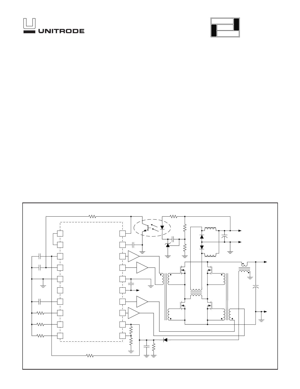
SIMPLIFIED APPLICATION DIAGRAM
1 EAN
UCC3895
EAP 270
2 EAOUT
SS/DISB 19
3 RAMP
OUTA 18
4 REF
OUTB 17
5 GND
PGND 16
6 SYNC
VCC 15
7 CT
OUTC 14
8 RT
OUTD 13
9 DELAB
CS 12
10 DELCD
ADS 11
Q1
VBIAS
A
B
VOUT
C
VIN
D
SLUS157A - DECEMBER 1999
UDG-98139
1 page 
PIN DESCRIPTIONS
ADS: Adaptive Delay Set. This function sets the ratio be-
tween the maximum and minimum programmed output
delay dead time. When the ADS pin is directly connected
to the CS pin, no delay modulation occurs. The maxi-
mum delay modulation occurs when ADS is grounded. In
this case, delay time is four times longer when CS = 0
than when CS = 2.0V (the Peak Current threshold), ADS
changes the output voltage on the delay pins DELAB
and DELCD by the following formula:
[ ]VDEL = 0.75 • (VCS −V ADS ) + 0. 5V
where VCS and VADS are in Volts. ADS must be limited to
between 0V and 2.5V and must be less than or equal to
CS. DELAB and DELCD also will be clamped to a mini-
mum of 0.5V.
EAOUT: Error Amplifier Output. It is also connected in-
ternally to the non-inverting input of the PWM compara-
tor and the no-load comparator. EAOUT is internally
clamped to the soft start voltage. The no-load compara-
tor shuts down the output stages when EAOUT falls be-
low 500mV, and allows the outputs to turn-on again
when EAOUT rises above 600mV.
CT: Oscillator Timing Capacitor. (Refer to Fig. 1, Oscilla-
tor Block Diagram) The UCC3895’s oscillator charges CT
via a programmed current. The waveform on CT is a
sawtooth, with a peak voltage of 2.35V. The approximate
oscillator period is calculated by the following formula:
tOSC
= 5 • RT • CT
48
+ 120 ns
where CT is in Farads, and RT is in Ohms and tOSC is in
seconds. CT can range from 100pF to 880pF. Please
note that a large CT and a small RT combination will re-
sult in extended fall times on the CT waveform. The in-
creased fall time will increase the SYNC pulse width,
hence limiting the maximum phase shift between OUTA,
OUTB and OUTC, OUTD outputs, which limits the maxi-
mum duty cycle of the converter.
CS: Current Sense. This is the inverting input of the Cur-
rent Sense comparator and the non-inverting input of the
Over-current comparator, and the ADS amplifier. The
current sense signal is used for cycle-by-cycle current
limiting in peak current mode control, and for overcurrent
protection in all cases with a secondary threshold for out-
put shutdown. An output disable initiated by an
overcurrent fault also results in a restart cycle, called
“soft stop”, with full soft start.
UCC1895
UCC2895
UCC3895
DELAB, DELCD: Delay Programming Between
Complementary Outputs. DELAB programs the dead
time between switching of OUTA and OUTB, and
DELCD programs the dead time between OUTC and
OUTD. This delay is introduced between complementary
outputs in the same leg of the external bridge. The
UCC3895 allows the user to select the delay, in which
the resonant switching of the external power stages
takes place. Separate delays are provided for the two
half-bridges to accommodate differences in resonant
capacitor charging currents. The delay in each stage is
set according to the following formula:
( )25 • 10 −12 • RDEL
t DELAY =
VDEL
+ 25ns
where VDEL is in Volts, and RDEL is in Ohms and tDELAY
is in seconds. DELAB and DELCD can source about
1mA maximum. Choose the delay resistors so that this
maximum is not exceeded. Programmable output delay
can be defeated by tying DELAB and/or DELCD to REF.
For an optimum performance keep stray capacitance on
these pins at <10pF.
EAP: The non-inverting input to the error amplifier.
EAN: The inverting input to the error amplifier.
GND: Chip ground for all circuits except the output
stages.
OUTA, OUTB, OUTC, OUTD: The 4 outputs are 100mA
complementary MOS drivers, and are optimized to drive
FET driver circuits. OUTA and OUTB are fully
complementary, (assuming no programmed delay). They
operate near 50% duty cycle and one-half the oscillating
frequency. OUTA and OUTB are intended to drive one
half-bridge circuit in an external power stage. OUTC and
OUTD will drive the other half-bridge and will have the
same characteristics as OUTA and OUTB. OUTC is
phase shifted with respect to OUTA, and OUTD is phase
shifted with respect to OUTB. Note that changing the
phase relationship of OUTC and OUTD with respect to
OUTA and OUTB requires other than the nominal 50%
duty ratio on OUTC and OUTD during those transients.
PGND: Output Stage Ground. To keep output switching
noise from critical analog circuits, the UCC3895 has 2
different ground connections. PGND is the ground
connection for the high-current output stages. Both GND
and PGND must be electrically tied together closely near
the IC. Also, since PGND carries high current, board
traces must be low impedance.
5
5 Page | ||
| Páginas | Total 10 Páginas | |
| PDF Descargar | [ Datasheet UCC1895.PDF ] | |
Hoja de datos destacado
| Número de pieza | Descripción | Fabricantes |
| UCC1890 | Off-Line Battery Charger Circuit | Texas Instruments |
| UCC1895 | BiCMOS Advanced Phase Shift PWM Controller | Unitrode |
| UCC1895 | UCC1895 UCC2895 UCC3895 BiCMOS Advanced Phase-Shift PWM Controller (Rev. P) | Texas Instruments |
| Número de pieza | Descripción | Fabricantes |
| SLA6805M | High Voltage 3 phase Motor Driver IC. |
Sanken |
| SDC1742 | 12- and 14-Bit Hybrid Synchro / Resolver-to-Digital Converters. |
Analog Devices |
|
DataSheet.es es una pagina web que funciona como un repositorio de manuales o hoja de datos de muchos de los productos más populares, |
| DataSheet.es | 2020 | Privacy Policy | Contacto | Buscar |