|
|
PDF FST32211 Data sheet ( Hoja de datos )
| Número de pieza | FST32211 | |
| Descripción | 40/48-Bit Bus Switch | |
| Fabricantes | Fairchild Semiconductor | |
| Logotipo | ||
Hay una vista previa y un enlace de descarga de FST32211 (archivo pdf) en la parte inferior de esta página. Total 6 Páginas | ||
|
No Preview Available !
April 2001
Revised July 2002
FST32211
40/48-Bit Bus Switch
General Description
The Fairchild Switch FST32211 provides up to 48-bits of
high-speed CMOS TTL-compatible bus switching. The low
On Resistance of the switch allows inputs to be connected
to outputs without adding propagation delay or generating
additional ground bounce noise.
The device can be organized as four 12-bit, two 24-bit, or
one 48-bit bus switch. When routed as a 40-bit bus switch,
the device can be organized as four 10-bit, two 20-bit or
one 40-bit bus switch. When OE1 is LOW, the switch is ON
and Port 1A is connected to Port 1B. When OE2 is LOW,
the switch is ON and Port 2A is connected to Port 2B.
When OE3 is LOW, the switch is ON and Port 3A is con-
nected to Port 3B. When OE4 is LOW, the switch is ON and
Port 4A is connected to Port 4B. When OE1, OE2, OE3, or
OE4 are HIGH, a high impedance state exists between the
A and B Ports.
Features
I 4Ω switch connection between two ports
I Minimal propagation delay through the switch
I Low lCC
I Zero bounce in flow-through mode
I Control inputs compatible with TTL level
I Packaged in plastic Fine Pitch Ball Grid Array (FBGA)
Ordering Code:
Order Number Package Number
Package Description
FST32211G
(Note 1)(Note 2)
BGA114A
114-Ball Fine-Pitch Ball Grid Array (FBGA), JEDEC MO-205, 5.5mm Wide
Note 1: Ordering code “G” indicates Trays.
Note 2: Devices also available in Tape and Reel. Specify by appending the suffix letter “X” to the ordering code.
Logic Diagram
© 2002 Fairchild Semiconductor Corporation DS500404
www.DataSheet4U.net
www.fairchildsemi.com
1 page 
AC Electrical Characteristics
Symbol
Parameter
TA = −40 °C to +85 °C,
CL = 50pF, RU = RD = 500Ω
VCC = 4.5 – 5.5V
VCC = 4.0V
Units
Conditions
Figure
Number
Min Max Min Max
tPHL, tPLH
Propagation Delay Bus to Bus
(Note 9)
0.25
0.25 ns VI = OPEN
Figures
1, 2
tPZH, tPZL
Output Enable Time
1.5 6.0
6.5 ns VI = 7V for tPZL
VI = OPEN for tPZH
Figures
1, 2
tPHZ, tPLZ
Output Disable Time
1.5 7.0
7.2 ns VI = 7V for tPLZ
VI = OPEN for tPHZ
Figures
1, 2
Note 9: This parameter is guaranteed by design but is not tested. The bus switch contributes no propagation delay other than the RC delay of the typical On
Resistance of the switch and the 50pF load capacitance, when driven by an ideal voltage source (zero output impedance).
Capacitance (Note 10)
Symbol
Parameter
Typ
CIN Control Pin Input Capacitance
3
CI/O Input/Output Capacitance
6
Note 10: TA = +25°C, f = 1 MHz, Capacitance is characterized but not tested.
Max
Units
pF
pF
Conditions
VCC = 5.0V
VCC, OE = 5.0V
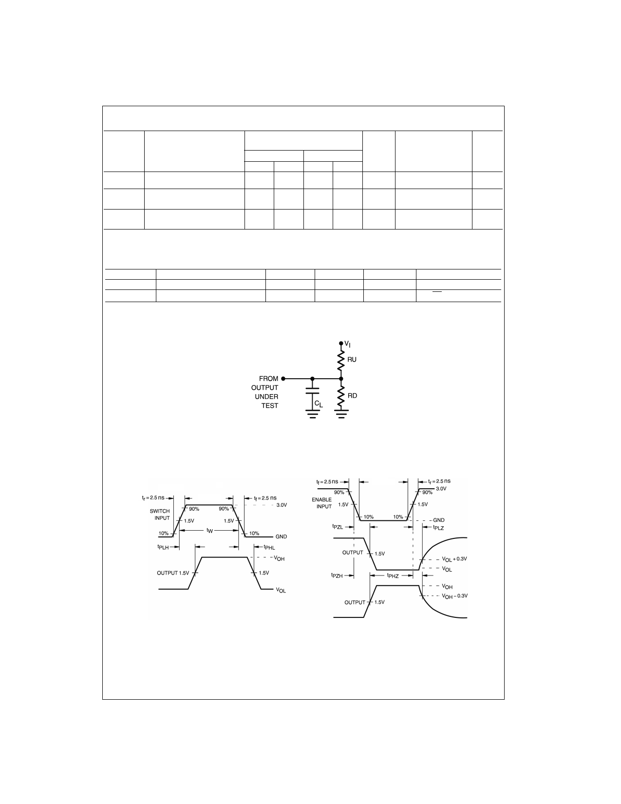
AC Loading and Waveforms
Note: Input driven by 50Ω source terminated in 50Ω
Note: CL includes load and stray capacitance
Note: Input PRR = 1.0 MHz, tW = 500 ns
FIGURE 1. AC Test Circuit
FIGURE 2. AC Waveforms
5
www.fairchildsemi.com
5 Page | ||
| Páginas | Total 6 Páginas | |
| PDF Descargar | [ Datasheet FST32211.PDF ] | |
Hoja de datos destacado
| Número de pieza | Descripción | Fabricantes |
| FST32211 | 40/48-Bit Bus Switch | Fairchild Semiconductor |
| FST32211G | 40/48-Bit Bus Switch | Fairchild Semiconductor |
| Número de pieza | Descripción | Fabricantes |
| SLA6805M | High Voltage 3 phase Motor Driver IC. |
Sanken |
| SDC1742 | 12- and 14-Bit Hybrid Synchro / Resolver-to-Digital Converters. |
Analog Devices |
|
DataSheet.es es una pagina web que funciona como un repositorio de manuales o hoja de datos de muchos de los productos más populares, |
| DataSheet.es | 2020 | Privacy Policy | Contacto | Buscar |
