|
|
|
PDF LTC3882 Data sheet ( Hoja de datos )
| Número de pieza | LTC3882 | |
| Descripción | Dual Output PolyPhase Step-Down DC/DC Voltage Mode Controller | |
| Fabricantes | Linear Technology | |
| Logotipo | ||
Hay una vista previa y un enlace de descarga de LTC3882 (archivo pdf) en la parte inferior de esta página. Total 30 Páginas | ||
|
No Preview Available !
LTC3882
Dual Output PolyPhase
Step-Down DC/DC Voltage Mode Controller
with Digital Power System Management
FEATURES
DESCRIPTION
n PMBus/I2C Compliant Serial Interface
– Monitor Voltage, Current, Temperature and Faults
– Digitally Programmable Voltage, Current Limit,
Soft-Start/Stop, Sequencing, Margining, AVP
and UV/OV Thresholds
n 3V ≤ VINSNS ≤ 38V, 0.5V ≤ VOUT ≤ 5.25V
n ±0.5% Output Voltage Accuracy
n Programmable PWM Frequency or External Clock
Synchronization from 250kHz to 1.25MHz
n Accurate PolyPhase® Current Sharing
n Internal EEPROM with Fault Logging
n IC Supply Range: 3V to 13.2V
n Resistor or Inductor DCR Current Sensing
n Optional Resistor Programming for Key Parameters
n 40-Pin (6mm × 6mm) QFN Package
APPLICATIONS
n High Current Distributed Power Systems
n Servers, Network and Storage Equipment
n Intelligent Energy Efficient Power Regulation
n Industrial/Telecom/ATE Systems
The LTC®3882 is a dual, PolyPhase DC/DC synchronous
step-down switching regulator controller with PMBus
compliant serial interface. It uses a constant frequency,
leading-edge modulation, voltage mode architecture for
excellent transient response and output regulation. Each
PWM channel can produce output voltages from 0.5V to
5.25V using a wide range of 3.3V compatible power stages,
including power blocks, DrMOS or discrete FET drivers.
Up to four LTC3882s can operate in parallel for 2-, 3-, 4-,
6- or 8-phase operation.
LTC3882 system configuration and monitoring is supported
by the LTpowerPlay™ software tool. The device’s serial
interface can be used to read back input voltage, output
voltage and current, temperature and fault status. A wide
range of operating parameters can be set via the digital
interface or stored in internal EEPROM for use at power
up. Switching frequency and phase, output voltage and
device address can also be programmed using external
configuration resistors.
L, LT, LTC, LTM, Linear Technology,the Linear logo and PolyPhase are registered trademarks
and LTpowerPlay is a trademark of Linear Technology Corporation. All other trademarks are the
property of their respective owners. Protected by U.S. Patents, including 5396245, 5859606,
6144194, 6937178, 7420359 and 7000125.
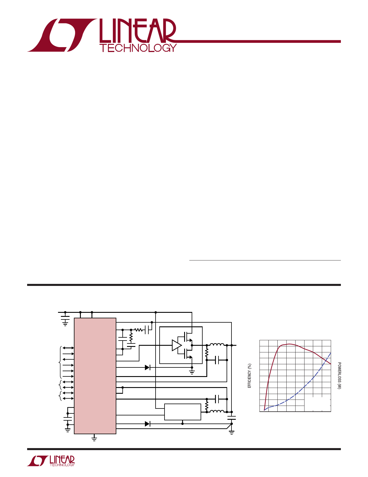
TYPICAL APPLICATION
VIN
7V TO 13.2V
TO/FROM
MCU
TO/FROM
EXTERNAL DEVICES
TO/FROM OTHER
OTHER PHASES
VCC VINSNS VSENSE0+
FB0
LTC3882
SDA
SCL
ALERT
RUN0
RUN1
WP
GPIO0
GPIO1
SHARE_CLK
SYNC
IAVG0
IAVG1
COMP0
COMP1
PWM0
TSNS0
ISENSE0+
ISENSE0–
VSENSE1+
ISENSE1–
ISENSE1+
PWM1
IAVG_GND
GND
TSNS1
VSENSE0–
FDMF5820A
PWM
VIN
SW
GND
VOUT
1V
80A
VIN FDMF5820A
PWM GND
SW
INDUCTORS: COOPER FP1007R1-R22
SOME DETAILS OMITTED FOR CLARITY
3882 TA01a
For more information www.linear.com/LTC3882
Efficiency and Power Loss vs
Load Current
92 13
91
90 11
89
88 9
87
86 7
85
84 5
83
82
VIN = 12V
3
81
VOUT = 1V
SYNC = 500kHz
80 1
0 10 20 30 40 50 60 70 80
LOAD CURRENT (A)
3882 TA01b
3882f
1
1 page 
LTC3882
E LECTRICAL CHARACTERISTICS The l denotes the specifications which apply over the specified operating
junction temperature range,
VSENSE1– = IAVG_GND = GND =
o0tVh,efrSwYNisCe=s5p0e0cikfHicza(teioxntesranraellaytdTrJiv=en2)5u°Cnl(eNsostoet2h)e.rwVCisCe=s5pVe,cVifSieENdS. E0+
=
VSENSE1+
=
1.8V,
VSENSE0–
=
SYMBOL
PARAMETER
CONDITIONS
MIN TYP MAX UNITS
VDD33 Linear Regulator
VDD33
Internal VDD33 Voltage
IDD33
VDD33 Current Limit
VDD25 Linear Regulator
VDD25
Internal VDD25 Voltage
IDD25
VDD25 Current Limit
PWM Control Loops
VCC ≥ 4.5V
VDD33 = 2.8V
VDD33 = 0V
l 3.2 3.3 3.4
85
40
2.25 2.5 2.75
95
V
mA
mA
V
mA
VINSNS
RVINSNS
VOUT_R0
VIN Sense Voltage Range
VINSNS Input Resistance
Range
Range
0
0
SMeatxPimoiunmt AVcOcUuTracy
(Note
7)
Range 0 Resolution
Range 0 LSB Step Size
0.6V ≤ VOUT ≤ 5V
0.6V ≤ VOUT ≤ 5V
3
278
5.25
±0.2
l –0.5
12
1.375
38
0.5
V
kΩ
V
%
%
Bits
mV
VOUT_R1
Range 1 Maximum VOUT
Range 1 Set Point Accuracy (Note 7)
Range 1 Resolution
Range 1 LSB Step Size
0.6V ≤ VOUT ≤ 2.5V
0.6V ≤ VOUT ≤ 2.5V
2.65
±0.2
l –0.5
0.5
12
0.6875
V
%
%
Bits
mV
IVSENSE
VLINEREG
AVP
VSENSE Input Current
VCC Line Regulation, No Output Servo
AVP Set Accuracy, ∆VOUT
Resolution
LSB Step Size
VVSSEENNSSEE+–
=
=
5.5V
0V
4.5V ≤ VCC ≤ 13.2V (See Test Circuit)
AVP = 10%, VOUT_COMMAND = 1.8V,
ISENSE Differential Step 3mV (20%) to 12mV (80%)
IOUT_OC_WARN_LIMIT at 15mV
–0.02
l –118
235
–335
0.02
–96
5
0.5
µA
µA
%/V
mV
Bits
%
AV(OL)
SR
Error Amplifier Open-Loop Voltage Gain
Error Amplifier Slew Rate
87 dB
9.5 V/µs
f0dB
ICOMP
RVSFB
Error Amplifier Bandwidth
Error Amplifier Output Current
Resistance Between VSENSE+ and FB
Sourcing
Sinking
Range 0
Range 1
30
–2.6
34
l 52 67 83
l 37 49 61
MHz
mA
mA
kΩ
kΩ
VISENSE
IISENSE
IAVG_VOS
ISENSE Differential Input Range
ISENSE± Input Current
IAVG Current Sense Offset
0V ≤ VPIN ≤ 5.5V
Referred to ISENSE Inputs
–1
l –600
±70
±0.1
±175
1
650
mV
µA
µV
µV
VSIOS
Slave Current Sharing Offset
Referred to ISENSE Inputs
±300
l –800
700
µV
µV
fSYNC
SYNC Frequency Accuracy
Input Voltage Supervisor
250kHz ≤ fSYNC ≤ 1.25MHz
l –10
10 %
NVON
Input ON/OFF Resolution
LSB Step Size
8 Bits
143 mV
VON_TOL
Input ON/OFF Threshold Accuracy
Output Voltage Supervisors
15V ≤ VIN_ON ≤ 35V
l –2
2%
NUVOV
Resolution
9 Bits
For more information www.linear.com/LTC3882
3882f
5
5 Page 
TYPICAL PERFORMANCE CHARACTERISTICS
LTC3882
Temperature ADC TUE
1.0
0.8
0.6
0.4
0.2
0
–0.2
–0.4
–0.6
–0.8
–1.0
–45 –25 –5 15 35 55 75 95 115
ACTUAL TEMPERATURE (°C)
3882 G22
SHARE_CLK Frequency vs
Temperature
110
105
100
95
90
–50 –30 –10 10 30 50 70
TEMPERATURE (°C)
90 110
3882 G23
IC Operating Current vs
Temperature
31.0
VCC = 14V
30.8
30.6
30.4
30.2
30.0
29.8
29.6
29.4
–40 –20
0 20 40 60 80
TEMPERATURE (°C)
100 120
3882 G24
PIN FUNCTIONS
COMP0/COMP1 (Pin 1/Pin 29): Error Amplifier Outputs.
PWM duty cycle increases with this control voltage. These
are true low impedance outputs and cannot be directly
connected together when active. For PolyPhase operation,
wiring FB to VDD33 will three-state the error amplifier output
of that channel, making it a slave. PolyPhase control is
then implemented in part by connecting all slave COMP
pins together to one master error amplifier output.
TSNS0/TSNS1 (Pin 2/Pin 3): External Temperature Sense
Inputs. The LTC3882 supports two methods of calcula-
tion of external temperature based on forward-biased P/N
junctions between these pins and GND.
BG0(EN0)/BG1(EN1) (Pin 6/Pin 28): PWM Multi-Function
Control Pins. These pins can be digitally programmed to
provide direct bottom FET control (BGn function) or PWM
enable control (ENn function), depending on external gate
driver requirements. These pins can also function as inputs
for three-state PWM protocol selection and should be left
open if not used.
TG0(PWM0)/TG1(PWM1) (Pin 7/Pin 27): PWM Multi-
Function Control Outputs. These pins can be digitally pro-
grammed to provide direct top FET control (TGn function)
or single-wire PWM switching control (PWMn function),
depending on external gate driver requirements.
VINSNS (Pin 4): VIN Supply Sense. Connect to the VIN
power supply to provide line feedforward compensation.
A change in VIN immediately modulates the input to the
PWM comparator and inversely changes the pulse width
to provide excellent transient line regulation and fixed
modulator voltage gain. An external lowpass filter can be
added to this pin to prevent noisy signals from affecting
the loop gain.
IAVG_GND (Pin 5): IAVG Ground Reference. The same
IAVG_GND should be shared between all channels of a
PolyPhase rail and connected to system ground at a single
point. IAVG_GND may be wired directly to GND on ICs that
do not share phases with other chips.
SYNC (Pin 8): External Clock Synchronization Input and
Open-Drain Output. If desired, an external clock can be
applied to this pin to synchronize the internal PWM chan-
nels. If the LTC3882 is configured as a clock master, this
pin will also pull to ground at the selected PWM switching
frequency with a 125ns pulse width. A pull-up resistor to
3.3V is required in the application if SYNC is driven by any
LTC3882. Minimize the capacitance on this line to ensure
its time constant is fast enough for the application.
SCL (Pin 9): Serial Bus Clock Input. A pull-up resistor to
3.3V is required in the application.
SDA (Pin 10): Serial Bus Data Input and Output. A pull-up
resistor to 3.3V is required in the application.
For more information www.linear.com/LTC3882
3882f
11
11 Page | ||
| Páginas | Total 30 Páginas | |
| PDF Descargar | [ Datasheet LTC3882.PDF ] | |
Hoja de datos destacado
| Número de pieza | Descripción | Fabricantes |
| LTC3880 | Dual Output PolyPhase Step-Down DC/DC Controller | Linear Technology |
| LTC3880-1 | Dual Output PolyPhase Step-Down DC/DC Controller | Linear Technology |
| LTC3882 | Dual Output PolyPhase Step-Down DC/DC Voltage Mode Controller | Linear Technology |
| Número de pieza | Descripción | Fabricantes |
| SLA6805M | High Voltage 3 phase Motor Driver IC. |
Sanken |
| SDC1742 | 12- and 14-Bit Hybrid Synchro / Resolver-to-Digital Converters. |
Analog Devices |
|
DataSheet.es es una pagina web que funciona como un repositorio de manuales o hoja de datos de muchos de los productos más populares, |
| DataSheet.es | 2020 | Privacy Policy | Contacto | Buscar |