|
|
|
PDF STM32F302VD Data sheet ( Hoja de datos )
| Número de pieza | STM32F302VD | |
| Descripción | ARM Cortex-M4 32b MCU+FPU | |
| Fabricantes | STMicroelectronics | |
| Logotipo | ||
Hay una vista previa y un enlace de descarga de STM32F302VD (archivo pdf) en la parte inferior de esta página. Total 30 Páginas | ||
|
No Preview Available !
STM32F302xD STM32F302xE
ARM® Cortex®-M4 32b MCU+FPU, up to 512KB Flash, 64KB
SRAM, FMC, 2 ADCs, 1 DAC ch., 4 comp, 2 Op-Amp, 2.0-3.6 V
Datasheet - production data
Features
• Core: ARM® Cortex®-M4 32-bit CPU with
72 MHz FPU, single-cycle multiplication and
HW division, DSP instruction and MPU
(memory protection unit)
• Operating conditions:
– VDD, VDDA voltage range: 2.0 V to 3.6 V
• Memories
– Up to 512 Kbytes of Flash memory
– 64 Kbytes of SRAM, with HW parity check
implemented on the first 32 Kbytes.
– Flexible memory controller (FMC) for static
memories, with four Chip Select
• CRC calculation unit
• Reset and supply management
– Power-on/Power-down reset (POR/PDR)
– Programmable voltage detector (PVD)
– Low power modes: Sleep, Stop and Standby
– VBAT supply for RTC and backup registers
• Clock management
– 4 to 32 MHz crystal oscillator
– 32 kHz oscillator for RTC with calibration
– Internal 8 MHz RC with x 16 PLL option
– Internal 40 kHz oscillator
• Up to 115 fast I/Os
– All mappable on external interrupt vectors
– Several 5 V-tolerant
• Interconnect matrix
• 12-channel DMA controller
• Two ADCs 0.20 µs (up to 18 channels) with
selectable resolution of 12/10/8/6 bits, 0 to
3.6 V conversion range, separate analog
supply from 2.0 to 3.6 V
• One 12-bit DAC channels with analog supply
from 2.4 to 3.6 V
• Four ultra-fast rail-to-rail analog comparators
with analog supply from 2.0 to 3.6 V
• Two operational amplifiers that can be used in
PGA mode, all terminals accessible with analog
supply from 2.4 to 3.6 V
• Up to 24 capacitive sensing channels supporting
touchkey, linear and rotary touch sensors
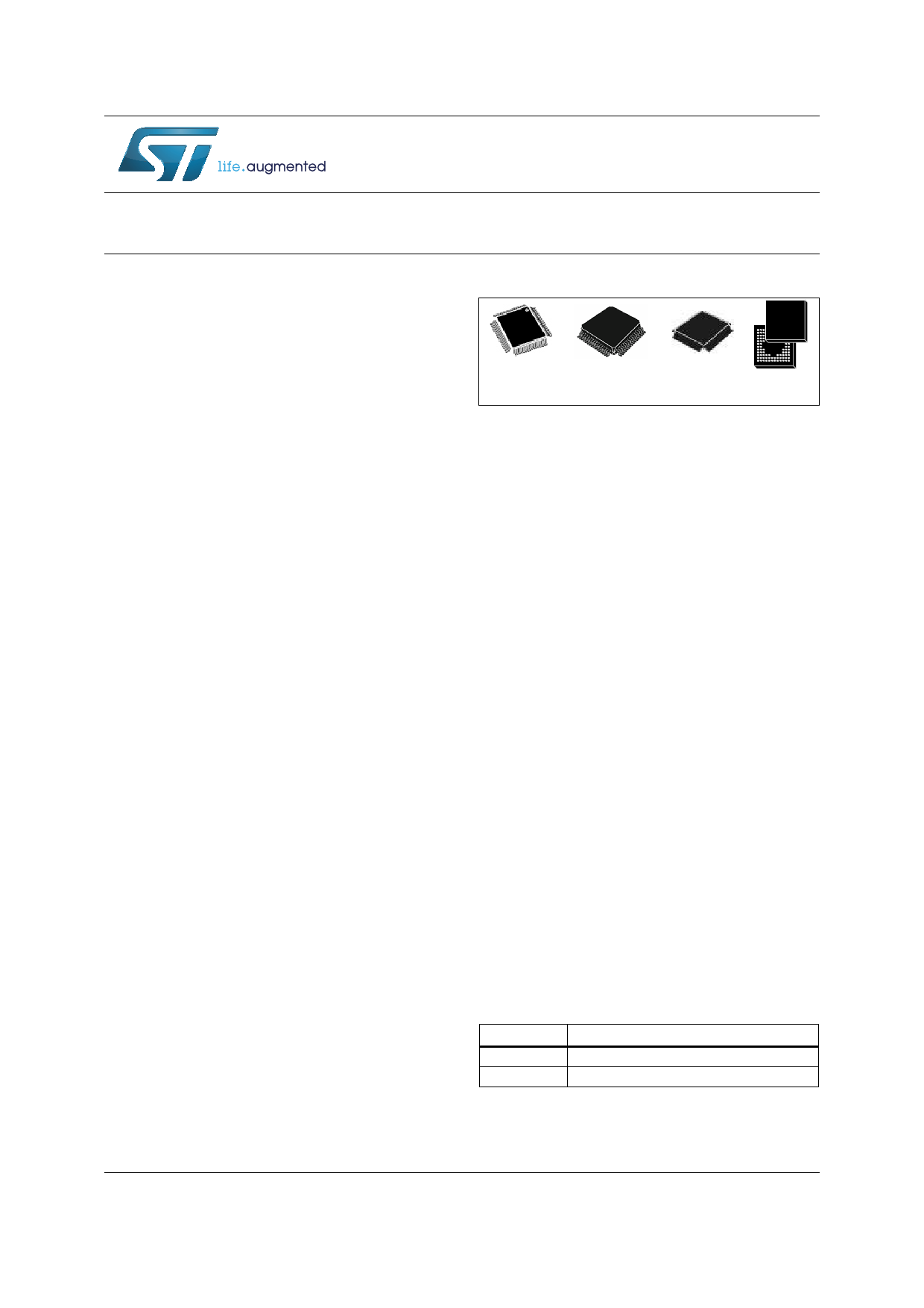
)%*$
LQFP64
(10 × 10 mm)
LQFP100
(14 × 14 mm)
LQFP144
(20 x 20 mm)
UFBGA100
(7 x 7 mm)
• Up to 11 timers
– One 32-bit timer and two 16-bit timers with
up to four IC/OC/PWM or pulse counter and
quadrature (incremental) encoder input
– One 16-bit 6-channel advanced-control
timers, with up to six PWM channels,
deadtime generation and emergency stop
– One 16-bit timer with two IC/OCs, one
OCN/PWM, deadtime generation and
emergency stop
– Two 16-bit timers with IC/OC/OCN/PWM,
deadtime generation and emergency stop
– Two watchdog timers (independent, window)
– One SysTick timer: 24-bit downcounter
– One 16-bit basic timers to drive the DAC
• Calendar RTC with Alarm, periodic wakeup
from Stop/Standby
• Communication interfaces
– CAN interface (2.0B Active)
– Three I2C Fast mode plus (1 Mbit/s) with
20 mA current sink, SMBus/PMBus, wakeup
from STOP
– Up to five USART/UARTs (ISO 7816
interface, LIN, IrDA, modem control)
– Up to four SPIs, 4 to 16 programmable bit
frames, two with multiplexed half/full duplex
I2S interface
– USB 2.0 full speed interface with LPM
support
– Infrared transmitter
• SWD, Cortex®-M4 with FPU ETM, JTAG
• 96-bit unique ID
Reference
STM32F302xD
STM32F302xE
Table 1. Device summary
Part number
STM32F302RD, STM32F302VD, STM32F302ZD.
STM32F302RE, STM32F302VE, STM32F302ZE.
April 2015
This is information on a product in full production.
DocID026900 Rev 2
1/175
www.st.com
1 page 
STM32F302xD STM32F302xE
List of tables
List of tables
Table 1.
Table 2.
Table 3.
Table 4.
Table 5.
Table 6.
Table 7.
Table 8.
Table 9.
Table 10.
Table 11.
Table 12.
Table 13.
Table 14.
Table 15.
Table 16.
Table 17.
Table 18.
Table 19.
Table 20.
Table 21.
Table 22.
Table 23.
Table 24.
Table 25.
Table 26.
Table 27.
Table 28.
Table 29.
Table 30.
Table 31.
Table 32.
Table 33.
Table 34.
Table 35.
Table 36.
Table 37.
Table 38.
Table 39.
Table 40.
Table 41.
Table 42.
Table 43.
Table 44.
Table 45.
Table 46.
Device summary . . . . . . . . . . . . . . . . . . . . . . . . . . . . . . . . . . . . . . . . . . . . . . . . . . . . . . . . . . 1
STM32F302xD/E family device features and peripheral counts . . . . . . . . . . . . . . . . . . . . . 12
External analog supply values for analog peripherals . . . . . . . . . . . . . . . . . . . . . . . . . . . . 16
STM32F302xD/E peripheral interconnect matrix . . . . . . . . . . . . . . . . . . . . . . . . . . . . . . . . 17
Timer feature comparison . . . . . . . . . . . . . . . . . . . . . . . . . . . . . . . . . . . . . . . . . . . . . . . . . . 24
Comparison of I2C analog and digital filters . . . . . . . . . . . . . . . . . . . . . . . . . . . . . . . . . . . . 27
STM32F302xD/E I2C implementation . . . . . . . . . . . . . . . . . . . . . . . . . . . . . . . . . . . . . . . . 28
USART features . . . . . . . . . . . . . . . . . . . . . . . . . . . . . . . . . . . . . . . . . . . . . . . . . . . . . . . . . 29
STM32F302xD/E SPI/I2S implementation . . . . . . . . . . . . . . . . . . . . . . . . . . . . . . . . . . . . . 30
Capacitive sensing GPIOs available on STM32F302xD/E devices . . . . . . . . . . . . . . . . . . 32
Number of capacitive sensing channels available on
STM32F302xD/E devices . . . . . . . . . . . . . . . . . . . . . . . . . . . . . . . . . . . . . . . . . . . . . . . . . . 32
Legend/abbreviations used in the pinout table . . . . . . . . . . . . . . . . . . . . . . . . . . . . . . . . . . 38
STM32F302xD/E pin definitions . . . . . . . . . . . . . . . . . . . . . . . . . . . . . . . . . . . . . . . . . . . . . 38
STM32F302xD/E alternate function mapping . . . . . . . . . . . . . . . . . . . . . . . . . . . . . . . . . . . 48
Memory map, peripheral register boundary addresses . . . . . . . . . . . . . . . . . . . . . . . . . . . 60
Voltage characteristics . . . . . . . . . . . . . . . . . . . . . . . . . . . . . . . . . . . . . . . . . . . . . . . . . . . . 66
Current characteristics . . . . . . . . . . . . . . . . . . . . . . . . . . . . . . . . . . . . . . . . . . . . . . . . . . . . 67
Thermal characteristics. . . . . . . . . . . . . . . . . . . . . . . . . . . . . . . . . . . . . . . . . . . . . . . . . . . . 67
General operating conditions . . . . . . . . . . . . . . . . . . . . . . . . . . . . . . . . . . . . . . . . . . . . . . . 68
Operating conditions at power-up / power-down . . . . . . . . . . . . . . . . . . . . . . . . . . . . . . . . 69
Embedded reset and power control block characteristics. . . . . . . . . . . . . . . . . . . . . . . . . . 69
Programmable voltage detector characteristics . . . . . . . . . . . . . . . . . . . . . . . . . . . . . . . . . 70
Embedded internal reference voltage . . . . . . . . . . . . . . . . . . . . . . . . . . . . . . . . . . . . . . . . . 71
Internal reference voltage calibration values . . . . . . . . . . . . . . . . . . . . . . . . . . . . . . . . . . . 71
Typical and maximum current consumption from VDD supply at VDD = 3.6V . . . . . . . . . . . 73
Typical and maximum current consumption from the VDDA supply . . . . . . . . . . . . . . . . . . 74
Typical and maximum VDD consumption in Stop and Standby modes. . . . . . . . . . . . . . . . 75
Typical and maximum VDDA consumption in Stop and Standby modes. . . . . . . . . . . . . . . 75
Typical and maximum current consumption from VBAT supply. . . . . . . . . . . . . . . . . . . . . . 76
Typical current consumption in Run mode, code with data processing running
from Flash . . . . . . . . . . . . . . . . . . . . . . . . . . . . . . . . . . . . . . . . . . . . . . . . . . . . . . . . . . . . . 77
Typical current consumption in Sleep mode, code running from Flash or RAM . . . . . . . . . 78
Switching output I/O current consumption . . . . . . . . . . . . . . . . . . . . . . . . . . . . . . . . . . . . . 80
Peripheral current consumption . . . . . . . . . . . . . . . . . . . . . . . . . . . . . . . . . . . . . . . . . . . . . 81
Low-power mode wakeup timings . . . . . . . . . . . . . . . . . . . . . . . . . . . . . . . . . . . . . . . . . . . 83
High-speed external user clock characteristics. . . . . . . . . . . . . . . . . . . . . . . . . . . . . . . . . . 84
Low-speed external user clock characteristics . . . . . . . . . . . . . . . . . . . . . . . . . . . . . . . . . . 85
HSE oscillator characteristics . . . . . . . . . . . . . . . . . . . . . . . . . . . . . . . . . . . . . . . . . . . . . . . 86
LSE oscillator characteristics (fLSE = 32.768 kHz) . . . . . . . . . . . . . . . . . . . . . . . . . . . . . . . 88
HSI oscillator characteristics. . . . . . . . . . . . . . . . . . . . . . . . . . . . . . . . . . . . . . . . . . . . . . . . 90
LSI oscillator characteristics . . . . . . . . . . . . . . . . . . . . . . . . . . . . . . . . . . . . . . . . . . . . . . . . 91
PLL characteristics . . . . . . . . . . . . . . . . . . . . . . . . . . . . . . . . . . . . . . . . . . . . . . . . . . . . . . . 91
Flash memory characteristics . . . . . . . . . . . . . . . . . . . . . . . . . . . . . . . . . . . . . . . . . . . . . . . 92
Flash memory endurance and data retention . . . . . . . . . . . . . . . . . . . . . . . . . . . . . . . . . . . 92
Asynchronous non-multiplexed SRAM/PSRAM/NOR read timings . . . . . . . . . . . . . . . . . . 94
Asynchronous non-multiplexed SRAM/PSRAM/NOR read-NWAIT timings . . . . . . . . . . . . 94
Asynchronous non-multiplexed SRAM/PSRAM/NOR write timings . . . . . . . . . . . . . . . . . . 95
DocID026900 Rev 2
5/175
7
5 Page 
STM32F302xD STM32F302xE
Description
2 Description
The STM32F302xD/E family is based on the high-performance ARM® Cortex®-M4 32-bit
RISC core with FPU operating at a frequency of 72 MHz, and embedding a floating point
unit (FPU), a memory protection unit (MPU) and an embedded trace macrocell (ETM). The
family incorporates high-speed embedded memories (512 Kbyte of Flash memory, 64 Kbyte
of SRAM), a flexible memory controller (FMC) for static memories (SRAM, PSRAM, NOR
and NAND), and an extensive range of enhanced I/Os and peripherals connected to an
AHB and two APB buses.
The devices offer two fast 12-bit ADCs (5 Msps), four comparators, two operational
amplifiers, one DAC channel, a low-power RTC, up to two general-purpose 16-bit timers,
one general-purpose 32-bit timer, and one timer dedicated to motor control. They also
feature standard and advanced communication interfaces: up to three I2Cs, up to four SPIs
(two SPIs are with multiplexed full-duplex I2Ss), three USARTs, up to two UARTs, CAN and
USB. To achieve audio class accuracy, the I2S peripherals can be clocked via an external
PLL.
The STM32F302xD/E family operates in the -40 to +85°C and -40 to +105°C temperature
ranges from a 2.0 to 3.6 V power supply. A comprehensive set of power-saving mode allows
the design of low-power applications.
The STM32F302xD/E family offers devices in different packages ranging from 64 pins to
144 pins.
The set of included peripherals changes with the device chosen.
DocID026900 Rev 2
11/175
62
11 Page | ||
| Páginas | Total 30 Páginas | |
| PDF Descargar | [ Datasheet STM32F302VD.PDF ] | |
Hoja de datos destacado
| Número de pieza | Descripción | Fabricantes |
| STM32F302VB | ARM Cortex-M4F 32b MCU+FPU | STMicroelectronics |
| STM32F302VC | ARM Cortex-M4F 32b MCU+FPU | STMicroelectronics |
| STM32F302VD | ARM Cortex-M4 32b MCU+FPU | STMicroelectronics |
| STM32F302VE | ARM Cortex-M4 32b MCU+FPU | STMicroelectronics |
| Número de pieza | Descripción | Fabricantes |
| SLA6805M | High Voltage 3 phase Motor Driver IC. |
Sanken |
| SDC1742 | 12- and 14-Bit Hybrid Synchro / Resolver-to-Digital Converters. |
Analog Devices |
|
DataSheet.es es una pagina web que funciona como un repositorio de manuales o hoja de datos de muchos de los productos más populares, |
| DataSheet.es | 2020 | Privacy Policy | Contacto | Buscar |