|
|
|
PDF STP6N120K3 Data sheet ( Hoja de datos )
| Número de pieza | STP6N120K3 | |
| Descripción | N-channel MOSFET | |
| Fabricantes | STMicroelectronics | |
| Logotipo | ||
Hay una vista previa y un enlace de descarga de STP6N120K3 (archivo pdf) en la parte inferior de esta página. Total 17 Páginas | ||
|
No Preview Available !
STFW6N120K3, STP6N120K3,
STW6N120K3
N-channel 1200 V, 1.95 Ω typ., 6 A SuperMESH3™
Power MOSFET in TO-3PF, TO-220 and TO-247 packages
Datasheet — production data
Features
Order codes
VDSS
RDS(on)
max
ID
Ptot
STFW6N120K3 1200 V < 2.4 Ω 6 A 63 W
STP6N120K3 1200 V < 2.4 Ω 6 A 150 W
STW6N120K3 1200 V < 2.4 Ω 6 A 150 W
■ 100% avalanche tested
■ Extremely large avalanche performance
■ Gate charge minimized
■ Very low intrinsic capacitances
■ Zener-protected
Applications
■ Switching applications
Description
These SuperMESH3™ Power MOSFETs are the
result of improvements applied to
STMicroelectronics’ SuperMESH™ technology,
combined with a new optimized vertical structure.
These devices boast an extremely low on-
resistance, superior dynamic performance and
high avalanche capability, rendering them suitable
for the most demanding applications.
3
2
1
TO-3PF
TAB
3
2
1
TO-220
3
2
1
TO-247
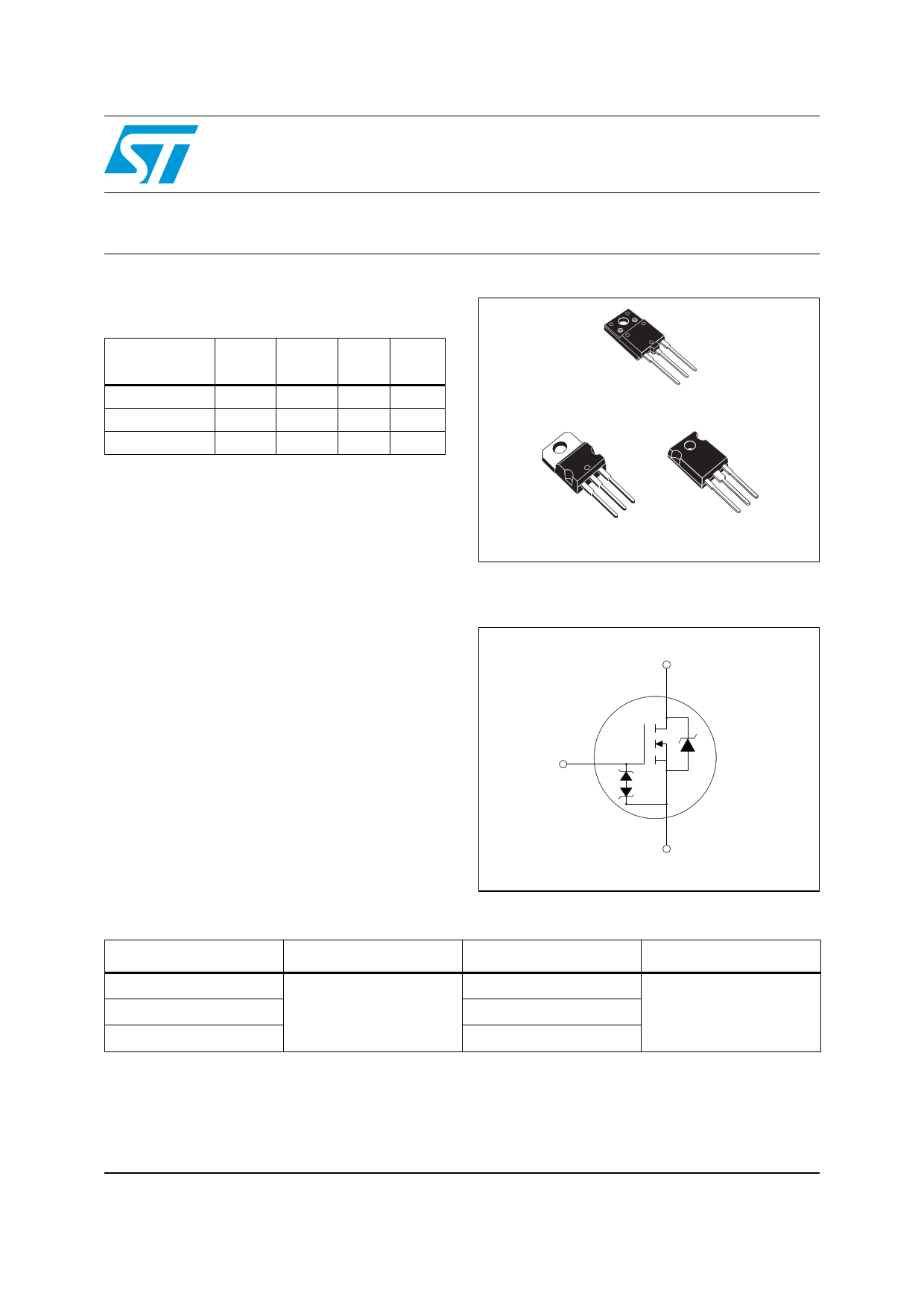
Figure 1. Internal schematic diagram
D(2,TAB)
G(1)
S(3)
AM01476v1
Table 1. Device summary
Order codes
STFW6N120K3
STP6N120K3
STW6N120K3
Marking
6N120K3
Package
TO-3PF
TO-220
TO-247
Packaging
Tube
November 2012
This is information on a product in full production.
Doc ID 15572 Rev 3
1/17
www.st.com
17
1 page 
STFW6N120K3, STP6N120K3, STW6N120K3
Electrical characteristics
Table 6. Switching times on/off
Symbol
Parameter
Test conditions
td(on)
tr
td(off)
tf
Turn-on delay time
Rise time
Turn-off-delay time
Fall time
VDD = 600 V, ID = 3.6 A,
RG = 4.7 Ω, VGS = 10 V
(see Figure 19)
Min. Typ. Max. Unit
30 ns
12 ns
--
58 ns
32 ns
Table 7.
Symbol
Source drain diode
Parameter
Test conditions
Min. Typ. Max. Unit
ISD
ISDM (1)
VSD (2)
Source-drain current
Source-drain current (pulsed)
Forward on voltage
ISD = 5 A, VGS = 0
6A
--
20 A
- -- 1.6 V
trr
Qrr
IRRM
Reverse recovery time
Reverse recovery charge
Reverse recovery current
ISD = 7.2 A, di/dt = 100 A/µs 580 ns
VDD = 60 V TJ = 25 °C (see
-
7
- µC
Figure 24)
25 A
trr
Qrr
IRRM
Reverse recovery time
Reverse recovery charge
Reverse recovery current
ISD = 7.2 A, di/dt = 100 A/µs 840 ns
VDD = 60 V, TJ = 150 °C
- 9 - µC
(see Figure 24)
22 A
1. Pulse width limited by safe operating area.
2. Pulsed: Pulse duration = 300 µs, duty cycle 1.5%
Table 8. Gate-source Zener diode
Symbol
Parameter
Test conditions
V(BR)GSO
Gate-source breakdown
voltage
IGS = ± 1 mA (ID=0)
Min. Typ. Max. Unit
30 - V
The built-in back-to-back Zener diodes have specifically been designed to enhance not only
the device’s ESD capability, but also to make them safely absorb possible voltage transients
that may occasionally be applied from gate to source. In this respect the Zener voltage is
appropriate to achieve an efficient and cost-effective intervention to protect the device’s
integrity. These integrated Zener diodes thus avoid the usage of external components.
Doc ID 15572 Rev 3
5/17
5 Page 
STFW6N120K3, STP6N120K3, STW6N120K3
Figure 25. TO-3PF drawing
L3
L
A
C
Dia
L2
Package mechanical data
D
E
D1
L6
F2(3x)
L7
F(3x)
G1
HG
R
L5 N
L4
7627132_C
Doc ID 15572 Rev 3
11/17
11 Page | ||
| Páginas | Total 17 Páginas | |
| PDF Descargar | [ Datasheet STP6N120K3.PDF ] | |
Hoja de datos destacado
| Número de pieza | Descripción | Fabricantes |
| STP6N120K3 | N-channel MOSFET | STMicroelectronics |
| Número de pieza | Descripción | Fabricantes |
| SLA6805M | High Voltage 3 phase Motor Driver IC. |
Sanken |
| SDC1742 | 12- and 14-Bit Hybrid Synchro / Resolver-to-Digital Converters. |
Analog Devices |
|
DataSheet.es es una pagina web que funciona como un repositorio de manuales o hoja de datos de muchos de los productos más populares, |
| DataSheet.es | 2020 | Privacy Policy | Contacto | Buscar |