|
|
|
PDF 25P10 Data sheet ( Hoja de datos )
| Número de pieza | 25P10 | |
| Descripción | 1 Mbit Low Voltage Paged Flash Memory | |
| Fabricantes | STMicroelectronics | |
| Logotipo | ||
Hay una vista previa y un enlace de descarga de 25P10 (archivo pdf) en la parte inferior de esta página. Total 21 Páginas | ||
|
No Preview Available !
M25P10
1 Mbit Low Voltage Paged Flash Memory
With 20 MHz Serial SPI Bus Interface
PRELIMINARY DATA
s 1 Mbit PAGED Flash Memory
s 128 BYTE PAGE PROGRAM IN 3 ms TYPICAL
s 256 Kbit SECTOR ERASE IN 1 s TYPICAL
s BULK ERASE IN 2 s TYPICAL
s SINGLE 2.7 V to 3.6 V SUPPLY VOLTAGE
s SPI BUS COMPATIBLE SERIAL INTERFACE
s 20 MHz CLOCK RATE AVAILABLE
s SUPPORTS POSITIVE CLOCK SPI MODES
s DEEP POWER DOWN MODE (1 µA TYPICAL)
s ELECTRONIC SIGNATURE
s 10,000 ERASE/PROG CYCLES PER SECTOR
s 20 YEARS DATA RETENTION
s –40 TO 85°C TEMPERATURE RANGE
DESCRIPTION
The M25P10 is an 1 Mbit Paged Flash Memory
fabricated with STMicroelectronics High
Endurance CMOS technology. The memory is
accessed by a simple SPI bus compatible serial
interface. The bus signals are a serial clock input
(C), a serial data input (D) and a serial data output
(Q).
The device connected to the bus is selected when
the chip select input (S) goes low. Data is clocked
in during the low to high transition of clock C, data
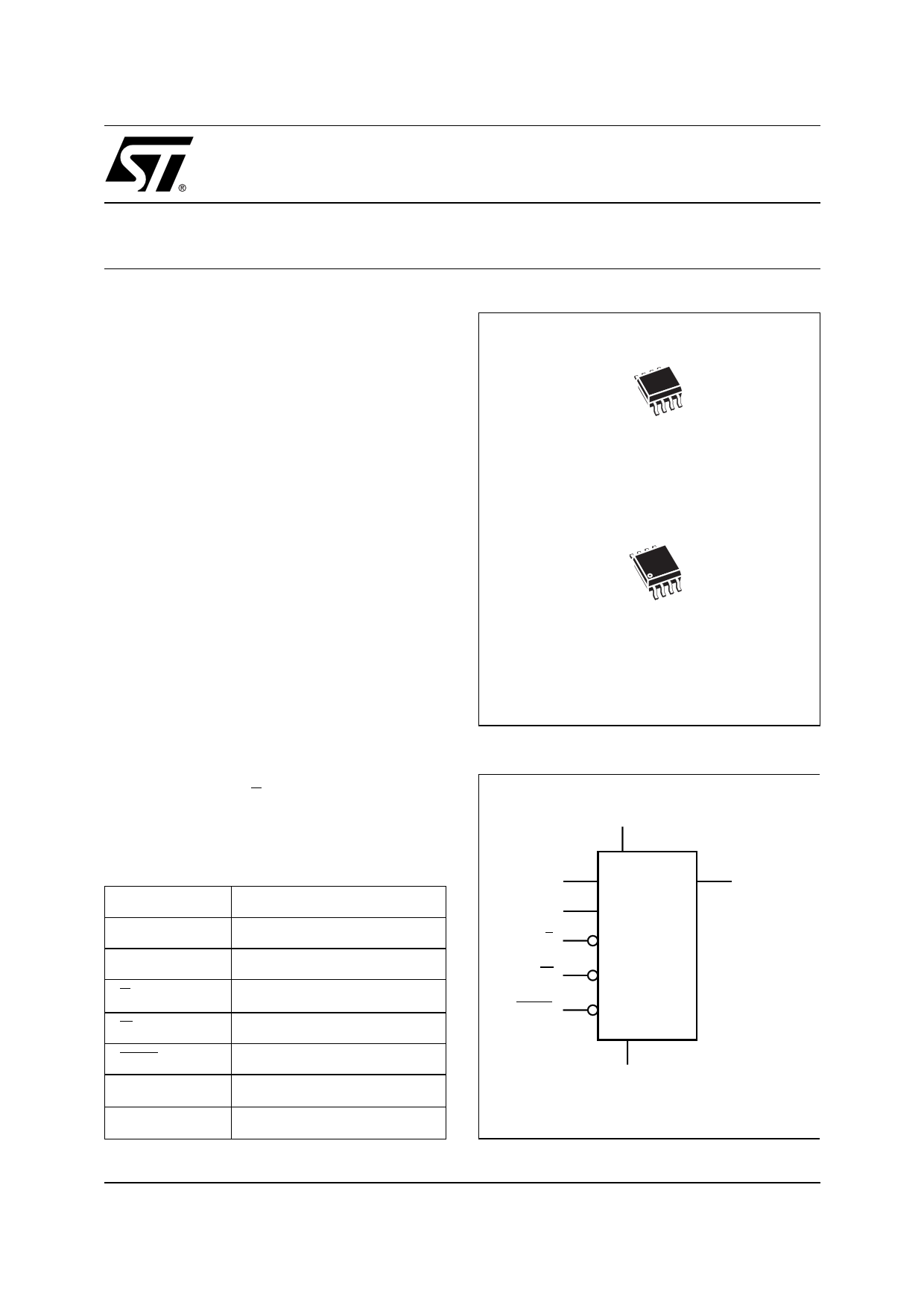
8
1
SO8 (MN)
150 mil width
8
1
SO8 (MW)
200 mil width
Figure 1. Logic Diagram
VCC
Table 1. Signal Names
C Serial Clock
D Serial Data Input
Q Serial Data Output
S Chip Select
W Write Protect
HOLD
Hold
VCC Supply Voltage
VSS Ground
D
C
S
W
HOLD
M25P10
VSS
Q
AI03744
June 2000
This is preliminary information on a new product now in development or undergoing evaluation. Details are subject to change without notice.
1/21
1 page 
Figure 6. Block Diagram
HOLD
W
S
C
D
Q
Control Logic
I/O Shift Register
High Voltage
Generator
Address Register
and Counter
Data
Register
1FF80h
Status
1FFFFh
An
0000h
An + 7Fh
128 Bytes
X Decoder
007Fh
M25P10
Size of the
Read only
Memory
area
AI03747
Table 5. Protected Area Sizes
BP1
BP0
00
01
10
11
Software Protected Area
none
Upper quarter = Sector 3
Upper half = Sectors 2 & 3
Whole memory= Sectors 0, 1, 2 & 3
5/21
5 Page 
M25P10
Figure 15. DP: Enter Deep Power Down Mode Sequence
S
01234567
tDP
C
INSTRUCTION
D
Stand-by Power Down Mode Deep Power Down Mode
AI03753
sets the Write Enable Latch (WEL) which allows
the execution of any further Bulk Erase. The Bulk
Erase instruction is entered by driving the Chip
select input (S) low, followed by the instruction
byte on Data In input (D).
The Chip Select input (S) must be driven low for
the entire duration of the sequence. The device
must be deselected just after the eighth bit of the
instruction byte has been latched in. If not, the
Bulk Erase instruction is not executed. As soon as
the device is deselected, the self-timed Bulk Erase
cycle (tBE) is initiated. While the Bulk Erase cycle
is in progress, the status register may be read to
check the WIP bit value. WIP is high during the
self-timed Bulk Erase cycle and is low when it is
completed. When the cycle is completed, the write
enable latch (WEL) is reset.
The Bulk Erase instruction is internally taken into
account if, and only if, (BP0, BP1) = (0,0). In other
words, the Bulk Erase instruction is ignored if at
least one Sector is software protected. In this case
the Bulk Erase instruction is discarded and none of
the Sectors are erased.
The timing sequence is shown in Figure 14.
Enter Deep Power Down Mode (DP)
After Power-on, when S is high, the memory is
deselected, the Q output pin is at high impedance
and the device is in the Standby Power Mode state
(ICC1). Under this state, the Memory waits for a
select condition and is able to receive, decode and
execute all instructions.This mode is not the Deep
Power Down Mode which is entered by the way of
a specific instruction. The purpose of the Deep
Power down mode is to drastically reduce the
standby current from ICC1 to ICC2 (see Table 10).
Once the device has entered the Deep Power
Down Mode, all instructions are ignored except the
RES instruction which releases the part from this
Figure 16. RES: Release from Deep Power Down Mode and Read Electronic Signature Sequence
S
0 1 2 3 4 5 6 7 8 9 10 28 29 30 31 32 33 34 35 36 37 38
C
INSTRUCTION
24 BIT ADDRESS
D
23 22 21
3210
HIGH IMPEDANCE
Q
DATA OUT (Electronic Signature)
76543210
MSB
Deep Power Down Mode Stand-by Power Down Mode
AI03755
11/21
11 Page | ||
| Páginas | Total 21 Páginas | |
| PDF Descargar | [ Datasheet 25P10.PDF ] | |
Hoja de datos destacado
| Número de pieza | Descripción | Fabricantes |
| 25P1 | Diode ( Rectifier ) | American Microsemiconductor |
| 25P10 | 1 Mbit Low Voltage Paged Flash Memory | STMicroelectronics |
| 25P10A | 1Mb 3V Serial Flash Embedded Memory | Micron |
| 25P10AV | M25P10AV | ST Microelectronics |
| Número de pieza | Descripción | Fabricantes |
| SLA6805M | High Voltage 3 phase Motor Driver IC. |
Sanken |
| SDC1742 | 12- and 14-Bit Hybrid Synchro / Resolver-to-Digital Converters. |
Analog Devices |
|
DataSheet.es es una pagina web que funciona como un repositorio de manuales o hoja de datos de muchos de los productos más populares, |
| DataSheet.es | 2020 | Privacy Policy | Contacto | Buscar |