|
|
PDF AT86RF212B Data sheet ( Hoja de datos )
| Número de pieza | AT86RF212B | |
| Descripción | 700/800/900MHz Transceiver | |
| Fabricantes | ATMEL Corporation | |
| Logotipo |  |
|
Hay una vista previa y un enlace de descarga de AT86RF212B (archivo pdf) en la parte inferior de esta página. Total 30 Páginas | ||
|
No Preview Available !
Features
• Fully integrated 769 – 935MHz transceiver including:
- Chinese WPAN band from 779 to 787MHz
- European SRD band from 863 to 870MHz
- North American ISM band from 902 to 928MHz
- Japanese band from 915 to 930MHz
• Direct Sequence Spread Spectrum with different modulation and data rates:
- BPSK with 20 and 40kb/s, compliant to IEEE® 802.15.4-2003/2006/2011
- O-QPSK with 100 and 250kb/s, compliant to IEEE 802.15.4-2006/2011
- O-QPSK with 250kb/s, compliant to IEEE 802.15.4-2011
- O-QPSK with 200, 400, 500, and 1000kb/s PSDU data rate
• Flexible combination of frequency bands and data rates
• Industry leading link budget:
- Receiver sensitivity up to -110dBm
- Programmable TX output power up to +11dBm
• Ultra-low current consumption:
- SLEEP = 0.2µA
- TRX_OFF = 450µA
- RX_ON = 9.2mA
- BUSY_TX = 18.0mA
at TX output power +5dBm
• Ultra-low supply voltage (1.8V to 3.6V) with internal regulator
• Easy to use interface:
- Registers, frame buffer, and AES accessible through fast SPI
- Clock output with prescaler from radio transceiver
• Radio transceiver features:
- 128-byte FIFO (SRAM) for data buffering
- Fully integrated, fast settling PLL to support Frequency Hopping
- Battery monitor
- Adjustable receiver sensitivity
- Integrated TX/RX switch, LNA, and PLL loop filter
- Automatic VCO and filter calibration
- Integrated 16MHz crystal oscillator
• Special IEEE 802.15.4™-2011 hardware support:
- FCS computation and Clear Channel Assessment
- RSSI measurement, Energy Detection and Link Quality Indication
• MAC hardware accelerator:
- Automated acknowledgement and retransmission
- CSMA-CA and Listen Before Talk (LBT)
- Automatic address filtering and automated FCS check
• Extended feature set hardware support:
- AES 128-bit hardware accelerator
- Antenna Diversity
- RX/TX indication for external RF front end control
- True Random Number Generation for security application
• Optimized for low BoM Cost and ease of production:
- Few external components necessary (crystal, capacitors and antenna)
- Excellent ESD robustness
- Industrial temperature range from -40°C to +85°C
• I/O and packages:
- 32-pin Low-Profile QFN Package 5 x 5 x 0.9mm³
- RoHS/Fully Green
• Compliant to IEEE 802.15.4-2003/2006/2011
• Compliant to ETSI EN 300 220-1, and FCC 47 CFR Section 15.247
AT86RF212B
Low Power,
700/800/900MHz
Transceiver for
ZigBee,
IEEE 802.15.4,
6LoWPAN, and
ISM
Applications
AT86RF212B
42002E–MCU Wireless–02/2015
1
Rev. 42002E–MCU Wireless–02/2015
1 page 
AT86RF212B
The RF port DC values depend on the operating state; refer to Chapter 7. In TRX_OFF
state, when the analog front-end is disabled (see Section 7.1.2.3), the RF pins are
pulled to ground, preventing a floating voltage larger than 1.8V which is not allowed for
the internal circuitry.
In transmit mode, a control loop provides a common-mode voltage of 0.9V. Transistor
M0 is off, allowing the PA to set the common-mode voltage. The common-mode
capacitance at each pin to ground shall be < 100pF to ensure the stability of this
common-mode feedback loop.
In receive mode, the RF port provides a low-impedance path to ground when transistor
M0 (see Figure 1-2) pulls the inductor center tap to ground. A DC voltage drop of 20mV
across the on-chip inductor can be measured at the RF pins.
1.2.3 Crystal Oscillator Pins
XTAL1, XTAL2
The pin 26 (XTAL1) of Atmel AT86RF212B is the input of the reference oscillator
amplifier (XOSC), the pin 25 (XTAL2) is the output. A detailed description of the crystal
oscillator setup and the related XTAL1/XTAL2 pin configuration can be found in
Section 9.7.
When using an external clock reference signal, XTAL1 shall be used as input pin. For
further details, refer to Section 9.7.3.
1.2.4 Analog Pin Summary
Table 1-2. Analog Pin Behavior – DC Values.
Pin Values and Conditions
RFP/RFN
VDC = 0.9V (BUSY_TX)
VDC = 20mV (receive states)
VDC = 0mV (otherwise)
XTAL1/XTAL2
VDC = 0.9V at both pins
CPAR = 3pF
DVDD
VDC = 1.8V (all states, except SLEEP)
VDC = 0mV (otherwise)
AVDD
VDC = 1.8V (all states, except P_ON,
SLEEP, RESET, and TRX_OFF)
VDC = 0mV (otherwise)
Comments
DC level at pins RFP/RFN for various transceiver states.
AC coupling is required if a circuitry with a DC path to ground or
supply is used. Serial capacitance and capacitance of each pin
to ground must be < 100pF.
DC level at pins XTAL1/XTAL2 for various transceiver states.
Parasitic capacitance (CPAR) of the pins must be considered as
additional load capacitance to the crystal.
DC level at pin DVDD for various transceiver states.
Supply pins (voltage regulator output) for the digital 1.8V
voltage domain. The outputs shall be bypassed by 1µF.
DC level at pin AVDD for various transceiver states.
Supply pin (voltage regulator output) for the analog 1.8V
voltage domain. The outputs shall be bypassed by 1µF.
42002E–MCU Wireless–02/2015
5
5 Page 
AT86RF212B
5 Application Schematic
5.1 Basic Application Schematic
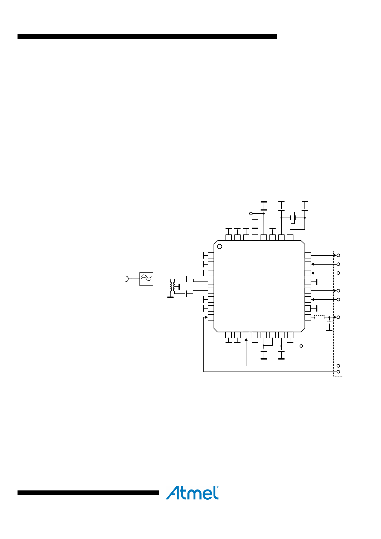
A basic application schematic of the Atmel AT86RF212B with a single-ended RF
connector is shown in Figure 5-1. The 50Ω single-ended RF input is transformed to the
100Ω differential RF port impedance using balun B1. The capacitors C1 and C2 provide
AC coupling of the RF input to the RF port. If the balun pins at the differential side
provide no DC path to ground and to the single-ended pin, the capacitors are not
necessary.
Regulatory rules like FCC 47 CFR Section 15.247 [5], ETSI EN 300 220-1 [6], and
ERC/REC 70-03 [7] may require an external filter F1, depending on used transmit
power levels.
Figure 5-1. Basic Application Schematic.
C1
RF
F1 B1
C2
CB2
VDD
CB1
CX1 XTAL
CX2
32 31 30 29 28 27 26 25
1 DIG3
2 DIG4
3 AVSS
4 RFP
5 RFN
6 AVSS
7 DVSS
8 /RST
AT86RF212B
IRQ 24
/SEL 23
MOSI 22
DVSS 21
MISO 20
SCLK 19
DVSS 18
CLKM 17
9 10 11 12 13 14 15 16
R1
C3
CB3 CB4
VDD
42002E–MCU Wireless–02/2015
The power supply decoupling capacitors (CB2, CB4) are connected to the external
analog supply pin 28 (EVDD) and external digital supply pin 15 (DEVDD). Capacitors
CB1 and CB3 are bypass capacitors for the integrated analog and digital voltage
regulators to ensure stable operation. All bypass capacitors should be placed as close
as possible to the pins and should have a low-resistance and low-inductance
connection to ground to achieve the best performance.
The crystal (XTAL), the two load capacitors (CX1, CX2), and the internal circuitry
connected to pins XTAL1 and XTAL2 form the crystal oscillator. To achieve the best
accuracy and stability of the reference frequency, large parasitic capacitances should
be avoided. Crystal lines should be routed as short as possible and not in proximity of
11
11 Page | ||
| Páginas | Total 30 Páginas | |
| PDF Descargar | [ Datasheet AT86RF212B.PDF ] | |
Hoja de datos destacado
| Número de pieza | Descripción | Fabricantes |
| AT86RF212 | Low Power 700/800/900 MHz Transceiver | ATMEL Corporation |
| AT86RF212B | 700/800/900MHz Transceiver | ATMEL Corporation |
| Número de pieza | Descripción | Fabricantes |
| SLA6805M | High Voltage 3 phase Motor Driver IC. |
Sanken |
| SDC1742 | 12- and 14-Bit Hybrid Synchro / Resolver-to-Digital Converters. |
Analog Devices |
|
DataSheet.es es una pagina web que funciona como un repositorio de manuales o hoja de datos de muchos de los productos más populares, |
| DataSheet.es | 2020 | Privacy Policy | Contacto | Buscar |
