|
|
PDF SH1106 Data sheet ( Hoja de datos )
| Número de pieza | SH1106 | |
| Descripción | 132 X 64 Dot Matrix OLED/PLED Segment/Common Driver | |
| Fabricantes | SINO WEALTH | |
| Logotipo |  |
|
Hay una vista previa y un enlace de descarga de SH1106 (archivo pdf) en la parte inferior de esta página. Total 30 Páginas | ||
|
No Preview Available !
SH1106
Preliminary
132 X 64 Dot Matrix OLED/PLED
Segment/Common Driver with Controller
Features
Support maximum 132 X 64 dot matrix panel
Embedded 132 X 64 bits SRAM
Operating voltage:
- Logic voltage supply: VDD1 = 1.65V - 3.5V
- DC-DC voltage supply: VDD2 = 3.0V – 4.2V
- OLED Operating voltage supply:
External VPP supply = 6.4V - 13.0V
Internal VPP generator = 6.4V - 9.0V
Maximum segment output current: 200μA
Maximum common sink current: 27mA
8-bit 6800-series parallel interface, 8-bit 8080-series
parallel interface, 3-wire & 4-wire serial peripheral
interface, 400KHz fast I2C bus interface
Programmable frame frequency and multiplexing ratio
Row re-mapping and column re-mapping (ADC)
Vertical scrolling
On-chip oscillator
Programmable Internal charge pump circuit output
256-step contrast control on monochrome passive OLED
panel
Low power consumption
- Sleep mode: <5μA
- VDD1=0V,VDD2=3.0V – 4.2V: <5μA
- VDD1,2=0V,VPP=3.0V – 4.2V: <5μA
Wide range of operating temperatures: -40 to +85°C
Available in COG form, thickness: 300μm
General Description
SH1106 is a single-chip CMOS OLED/PLED driver with controller for organic/polymer light emitting diode dot-matrix graphic
display system. SH1106 consists of 132 segments, 64 commons that can support a maximum display resolution of 132 X 64. It
is designed for Common Cathode type OLED panel.
SH1106 embeds with contrast control, display RAM oscillator and efficient DC-DC converter, which reduces the number of
external components and power consumption. SH1106 is suitable for a wide range of compact portable applications, such as
sub-display of mobile phone, calculator and MP3 player, etc.
1 V0.2
1 page 
OLED Drive Pads
Symbol
COM0,2,
- 60, 62
COM1,3
- 61,63
I/O
O
O
SEG0 - 131
O
Description
These pads are even Common signal output for OLED display.
These pads are odd Common signal output for OLED display.
These pads are Segment signal output for OLED display.
Test Pads
Symbol
TEST1-3
Dummy
I/O Description
I Test pad, internal pull low, no connection for user.
- These pads are not used. Keep floating.
SH1106
5 V0.2
5 Page 
SH1106
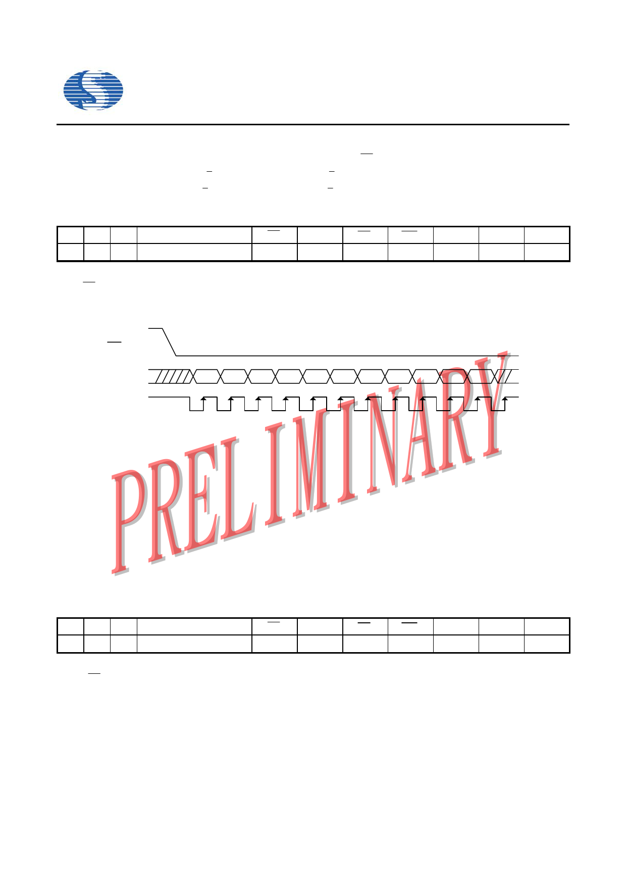
3 Wire Serial Interface (3-wire SPI)
The 3 wire serial interface consists of serial clock SCL, serial data SI, and CS . SI is shifted into an 9-bit shift register on every
rising edge of SCL in the order of D/ C , D7, D6, … and D0. The D/ C bit (first of the 9 bit) will determine the transferred data is
written to the display data RAM ( D/ C =1) or command register ( D/ C =0).
Table. 6
IM0 IM1 IM2
Type
CS
1 0 0 3-wire SPI
Pull Low
Note: “-” and Hz pin Must always be HIGH or LOW.
A0
Pull Low
CS signal could always pull low in SPI-bus application.
RD
-
WR D0
- SCL
D1 D2 to D7
SI (HZ)
CS
SI (D1)
SCL(D0)
D/C D7 D6 D5 D4 D3 D2 D1 D0 D/C D7
1 2 3 4 5 6 7 8 9 10 11
Figure. 2A -wire SPI data transfer
z When the chip is not active, the shift registers and the counter are reset to their initial statuses.
z Read is not possible while in serial interface mode.
z Caution is required on the SCL signal when it comes to line-end reflections and external noise. We recommend the
operation be rechecked on the actual equipment.
I2C-bus Interface
The SH1106 can transfer data via a standard I2C-bus and has slave mode only in communication. The command or RAM data
can be written into the chip and the status and RAM data can be read out of the chip.
IM0 IM1 IM2
Type
0 1 0 I2C Interface
CS A0 RD WR D0 D1 D2 to D7
Pull Low SA0
-
- SCL SDA (HZ)
Note: “-” and Hz pin Must always be HIGH or LOW.
CS signal could always pull low in I2C-bus application.
Characteristics of the I2C-bus
The I2C-bus is for bi-directional, two-line communication between different ICs or modules. The two lines are a serial data line
(SDA) and a serial clock line (SCL). Both lines must be connected to a positive supply via a pull-up resistor. Data transfer may
be initiated only when the bus is not busy.
Note: The positive supply of pull-up resistor must equal to the value of VDD1.
11 V0.2
11 Page | ||
| Páginas | Total 30 Páginas | |
| PDF Descargar | [ Datasheet SH1106.PDF ] | |
Hoja de datos destacado
| Número de pieza | Descripción | Fabricantes |
| SH1106 | 132 X 64 Dot Matrix OLED/PLED Segment/Common Driver | SINO WEALTH |
| Número de pieza | Descripción | Fabricantes |
| SLA6805M | High Voltage 3 phase Motor Driver IC. |
Sanken |
| SDC1742 | 12- and 14-Bit Hybrid Synchro / Resolver-to-Digital Converters. |
Analog Devices |
|
DataSheet.es es una pagina web que funciona como un repositorio de manuales o hoja de datos de muchos de los productos más populares, |
| DataSheet.es | 2020 | Privacy Policy | Contacto | Buscar |
