|
|
|
PDF MTP1302 Data sheet ( Hoja de datos )
| Número de pieza | MTP1302 | |
| Descripción | Power MOSFET ( Transistor ) | |
| Fabricantes | ON Semiconductor | |
| Logotipo | ||
Hay una vista previa y un enlace de descarga de MTP1302 (archivo pdf) en la parte inferior de esta página. Total 8 Páginas | ||
|
No Preview Available !
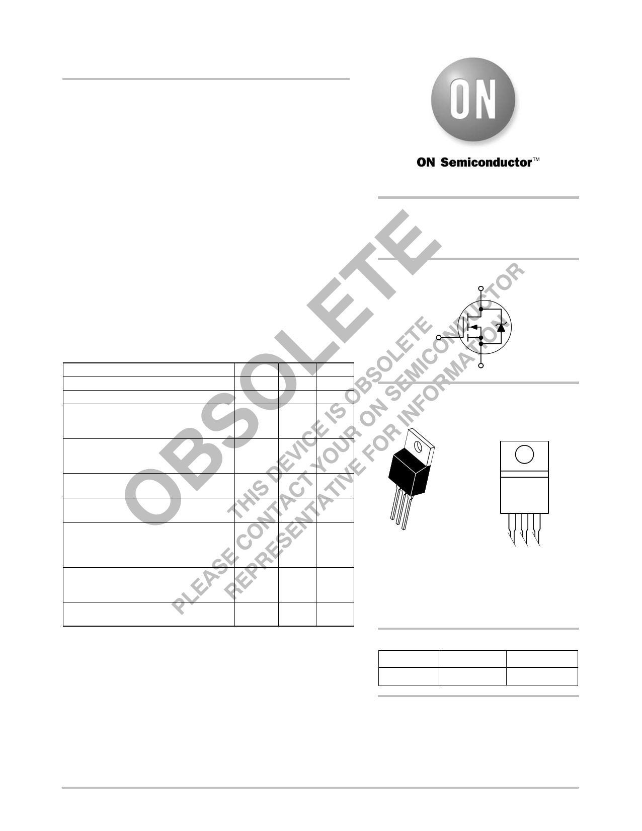
MTP1302
Preferred Device
Power MOSFET
42 Amps, 30 Volts
N−Channel TO−220
This Power MOSFET is designed to withstand high energy in the
avalanche and commutation modes. The energy efficient design also
offers a drain−to−source diode with a fast recovery time. Designed for
low voltage, high speed switching applications in power supplies,
converters and PWM motor controls, these devices are particularly
well suited for bridge circuits where diode speed and commutating
safe operating area are critical and offer additional safety margin
against unexpected voltage transients.
• Avalanche Energy Specified
• Source−to−Drain Diode Recovery Time Comparable to a
Discrete Fast Recovery Diode
• Diode Is Characterized for Use In Bridge Circuits
• IDSS and VDS(on) Specified at Elevated Temperature
MAXIMUM RATINGS (TC = 25°C unless otherwise noted)
Rating
Symbol Value
Drain−to−Source Voltage
Drain−to−Gate Voltage (RGS = 1.0 MΩ)
Gate−to−Source Voltage
− Continuous
− Non−Repetitive (tp ≤ 10 ms)
Drain Current − Continuous
Drain Current − Continuous @ 100°C
Drain Current − Single Pulse (tp ≤ 10 µs)
Total Power Dissipation
Derate above 25°C
VDSS
VDGR
VGS
VGSM
ID
ID
IDM
PD
30
30
± 20
± 20
42
20
126
74
0.592
Operating and Storage Temperature
Range
TJ, Tstg
− 55 to
150
Single Pulse Drain−to−Source Avalanche
Energy − Starting TJ = 25°C
(VDD = 25 Vdc, VGS = 10 Vdc, Peak
IL = 42 Apk, L = 0.25 mH, RG = 25 Ω)
Thermal Resistance
Junction to Case
Junction−to−Ambient
Maximum Lead Temperature for Soldering
Purposes, 1/8″ from Case for 5 seconds
EAS
RθJC
RθJA
TL
220
1.67
62.5
260
Unit
Vdc
Vdc
Vdc
Vpk
Adc
Apk
Watts
W/°C
°C
mJ
°C/W
°C
http://onsemi.com
42 AMPERES
30 VOLTS
RDS(on) = 22 mΩ
N−Channel
D
G
S
MARKING DIAGRAM
& PIN ASSIGNMENT
4
4 Drain
12
3
TO−220AB
CASE 221A
STYLE 5
MTP1302
LLYWW
1
Gate
3
Source
2
Drain
MTP1302
LL
Y
WW
= Device Code
= Location Code
= Year
= Work Week
ORDERING INFORMATION
Device
Package
Shipping
MTP1302
TO−220AB
50 Units/Rail
Preferred devices are recommended choices for future use
and best overall value.
© Semiconductor Components Industries, LLC, 2005
February, 2005 − Rev. XXX
1
Publication Order Number:
MTP1302/D
1 page 
MTP1302
14 18
12 15
QT
10
12
8.0 VGS
9.0
6.0
Q1
4.0
Q2
ID = 20 A
TJ = 25°C
6.0
2.0 Q3
3.0
VDS
00
0 2.0 4.0 6.0 8.0 10 12 14 16 18 20 22 24 26 28 30
QG, TOTAL GATE CHARGE (nC)
Figure 8. Gate−To−Source and Drain−To−Source
Voltage versus Total Charge
1000
VDD = 15 V
ID = 20 A
VGS = 10 V
TJ = 25°C
100
tf
tr
td(off)
10 td(on)
1.0
1.0
10
RG, GATE RESISTANCE (OHMS)
Figure 9. Resistive Switching Time
Variation versus Gate Resistance
100
DRAIN−TO−SOURCE DIODE CHARACTERISTICS
The switching characteristics of a MOSFET body diode
are very important in systems using it as a freewheeling or
commutating diode. Of particular interest are the reverse
recovery characteristics which play a major role in
determining switching losses, radiated noise, EMI and RFI.
System switching losses are largely due to the nature of
the body diode itself. The body diode is a minority carrier
device, therefore it has a finite reverse recovery time, trr, due
to the storage of minority carrier charge, QRR, as shown in
the typical reverse recovery wave form of Figure 15. It is this
stored charge that, when cleared from the diode, passes
through a potential and defines an energy loss. Obviously,
repeatedly forcing the diode through reverse recovery
further increases switching losses. Therefore, one would
like a diode with short trr and low QRR specifications to
minimize these losses.
The abruptness of diode reverse recovery effects the
amount of radiated noise, voltage spikes, and current
ringing. The mechanisms at work are finite irremovable
circuit parasitic inductances and capacitances acted upon by
high di/dts. The diode’s negative di/dt during ta is directly
controlled by the device clearing the stored charge.
However, the positive di/dt during tb is an uncontrollable
diode characteristic and is usually the culprit that induces
current ringing. Therefore, when comparing diodes, the
ratio of tb/ta serves as a good indicator of recovery
abruptness and thus gives a comparative estimate of
probable noise generated. A ratio of 1 is considered ideal and
values less than 0.5 are considered snappy.
Compared to ON Semiconductor standard cell density
low voltage MOSFETs, high cell density MOSFET diodes
are faster (shorter trr), have less stored charge and a softer
reverse recovery characteristic. The softness advantage of
the high cell density diode means they can be forced through
reverse recovery at a higher di/dt than a standard cell
MOSFET diode without increasing the current ringing or the
noise generated. In addition, power dissipation incurred
from switching the diode will be less due to the shorter
recovery time and lower switching losses.
20
18 TJ = 25°C
16
14
12
10
8.0
6.0
4.0
2.0
0
0.40 0.45 0.50 0.55 0.60 0.65 0.70 0.75 0.80 0.85 0.90
VSD, SOURCE−TO−DRAIN VOLTAGE (VOLTS)
Figure 10. Diode Forward Voltage versus Current
http://onsemi.com
5
5 Page | ||
| Páginas | Total 8 Páginas | |
| PDF Descargar | [ Datasheet MTP1302.PDF ] | |
Hoja de datos destacado
| Número de pieza | Descripción | Fabricantes |
| MTP1302 | TMOS POWER FET 42 AMPERES 30 VOLTS RDS(on) = 22 mohm | Motorola Semiconductors |
| MTP1302 | Power MOSFET ( Transistor ) | ON Semiconductor |
| MTP1306 | TMOS POWER FET 75 AMPERES 30 VOLTS RDS(on) = 0.0065 OHM | Motorola Semiconductors |
| Número de pieza | Descripción | Fabricantes |
| SLA6805M | High Voltage 3 phase Motor Driver IC. |
Sanken |
| SDC1742 | 12- and 14-Bit Hybrid Synchro / Resolver-to-Digital Converters. |
Analog Devices |
|
DataSheet.es es una pagina web que funciona como un repositorio de manuales o hoja de datos de muchos de los productos más populares, |
| DataSheet.es | 2020 | Privacy Policy | Contacto | Buscar |