|
|
|
PDF P3P85R01A Data sheet ( Hoja de datos )
| Número de pieza | P3P85R01A | |
| Descripción | 75 MHz to 200 MHz LVCMOS TIMING SAFE Peak EMI Reduction Device | |
| Fabricantes | ON Semiconductor | |
| Logotipo | ||
Hay una vista previa y un enlace de descarga de P3P85R01A (archivo pdf) en la parte inferior de esta página. Total 8 Páginas | ||
|
No Preview Available !
P3P85R01A
3.3V, 75 MHz to 200 MHz
LVCMOS TIMING SAFE]
Peak EMI Reduction Device
Functional Description
P3P85R01A is a versatile, 3.3 V, LVCMOS, wide frequency range,
TIMING SAFE Peak EMI reduction device. TIMING SAFE
technology is the ability to modulate a clock source with Spread
Spectrum technology and maintain synchronization with any
associated data path. Refer to Figure 3.
P3P85R01A has an SSEXTR pin that selects different frequency
deviations depending upon the value of the resistor connected between
this pin and GND.
P3P85R01A has a DLY_CTRL pin used for adjusting the
Input-Output clock delay, depending upon the value of capacitor
connected at this pin to GND. The DLY_CTRL output phase is
complementary to that of ModOUT clock. This signal enables better
EMI management.
P3P85R01A has a Bypass pin to bypass PLL. The device works
from 100 Hz to 200 MHz with a fixed input to output delay when in
Bypass mode.
P3P85R01A has a PLLOUT_DLY for adjusting the PLL Output
clock delay during power up time depending upon the value of
capacitor connected at this pin to VDD. During power up time,
ModOUT will be of the same frequency as CLKIN with a fixed input
to output delay.
General Features
• 1x, LVCMOS Peak EMI Reduction
• Input Frequency Range: 75 MHz − 200 MHz
• Output Frequency Range: 75 MHz − 200 MHz
• Analog Deviation Selection
• Analog Input−Output Delay Control
• Analog PLL Output Delay Control
• Low Cycle−to−Cycle Jitter
• Supply Voltage: 3.3 V ± 0.3 V
• 8 pin, WDFN, 2 mm x 2 mm (TDFN) Package
• Operating Temperature Range: 0°C to +70°C
• These Devices are Pb−Free, Halogen Free/BFR Free and are RoHS
Compliant
Application
• P3P85R01A is targeted for use in Displays, Giga LAN and SDRAM
applications.
http://onsemi.com
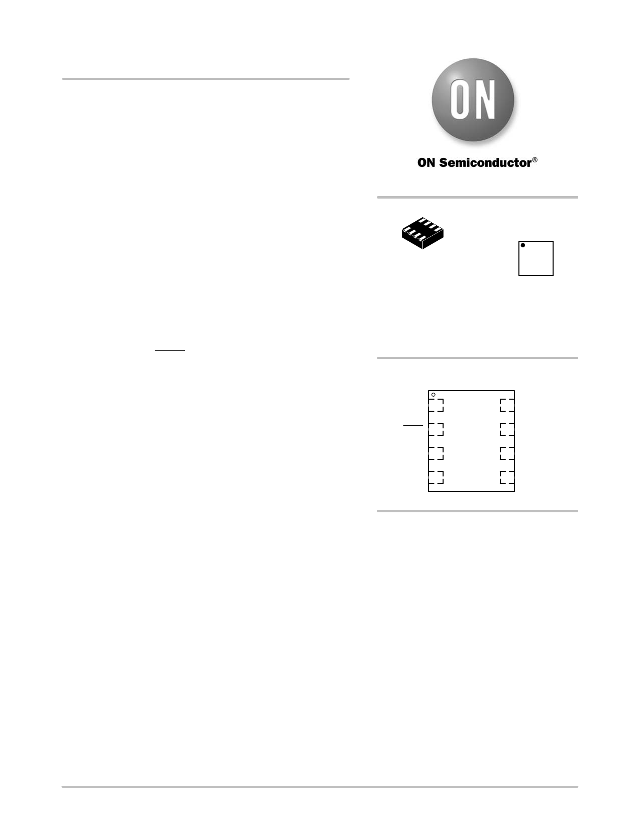
MARKING
DIAGRAMS
1
WDFN8
CASE 511AQ
1
DEMG
G
DE = Specific Device Code
M = Date Code
G = Pb−Free Device
(Note: Microdot may be in either location)
PIN CONFIGURATION
CLKIN 1
8 VDD
Bypass 2
7 PLLOUT_DLY
P3P85R01A
SSEXTR 3
6 DLY_CTRL
GND 4
5 ModOUT
ORDERING INFORMATION
See detailed ordering and shipping information in the package
dimensions section on page 7 of this data sheet.
© Semiconductor Components Industries, LLC, 2011
May, 2011 − Rev. 1
1
Publication Order Number:
P3P85R01A/D
1 page 
OUTPUT
OUTPUT
P3P85R01A
SWITCHING WAVEFORMS
VDD/2
t1
t2
VDD/2
VDD/2
Figure 4. Duty Cycle Timing
80%
80%
20%
20%
t3 t4
Figure 5. Output Rise/Fall Time
INPUT
OUTPUT
VDD/2
VDD/2
t5
Figure 6. Input − Output Propagation Delay
http://onsemi.com
5
5 Page | ||
| Páginas | Total 8 Páginas | |
| PDF Descargar | [ Datasheet P3P85R01A.PDF ] | |
Hoja de datos destacado
| Número de pieza | Descripción | Fabricantes |
| P3P85R01A | 75 MHz to 200 MHz LVCMOS TIMING SAFE Peak EMI Reduction Device | ON Semiconductor |
| Número de pieza | Descripción | Fabricantes |
| SLA6805M | High Voltage 3 phase Motor Driver IC. |
Sanken |
| SDC1742 | 12- and 14-Bit Hybrid Synchro / Resolver-to-Digital Converters. |
Analog Devices |
|
DataSheet.es es una pagina web que funciona como un repositorio de manuales o hoja de datos de muchos de los productos más populares, |
| DataSheet.es | 2020 | Privacy Policy | Contacto | Buscar |