|
|
|
PDF P3P8203A Data sheet ( Hoja de datos )
| Número de pieza | P3P8203A | |
| Descripción | General Purpose Peak EMI Reduction Device | |
| Fabricantes | ON Semiconductor | |
| Logotipo | ||
Hay una vista previa y un enlace de descarga de P3P8203A (archivo pdf) en la parte inferior de esta página. Total 6 Páginas | ||
|
No Preview Available !
P3P8203A
General Purpose Peak EMI
Reduction Device
Functional Description
P3P8203A is a versatile, 3.3 V LVCMOS Peak EMI reduction
device.
P3P8203A accepts an input clock either from a Fundamental
Crystal or from an external reference and locks on to it delivering a 1x
modulated clock.
P3P8203A has an SSEXTR pin to select different deviations
depending upon the value of an external resistor connected between
SSEXTR and GND.
P3P8203A operates with 3.3 V ± 0.3 V supply and is available in an
8 Pin, WDFN (2 mm X 2 mm) Package, over a temperature range of
0°C to +70°C.
Features
• 1x, LVCMOS Peak EMI Reduction
• Supports non-continuous input clock applications
• Input / output frequency range: 18 MHz − 36 MHz
• Analog Deviation Selection
• Supply Voltage: 3.3 V ± 0.3 V
• 8 pin, WDFN (2 mm X 2 mm) package
• Operating Temperature range: 0°C to +70°C
• These Devices are Pb−Free, Halogen Free/BFR Free and are RoHS
Compliant
Application
• P3P8203A is targeted for use in a broad range of note book and
desktop PCs and consumer electronic applications.
http://onsemi.com
MARKING
DIAGRAM
WDFN8
1 GJ MG
CASE 511AQ
G
1
GJ = Specific Device Code
M = Date Code
G = Pb−Free Device
(*Note: Microdot may be in either location)
PIN CONFIGURATION
XIN/CLKIN 1
XOUT 2
NC 3
GND 4
8 VDD
7 SSEXTR
6 NC
5 ModOUT
ORDERING INFORMATION
See detailed ordering and shipping information in the package
dimensions section on page 5 of this data sheet.
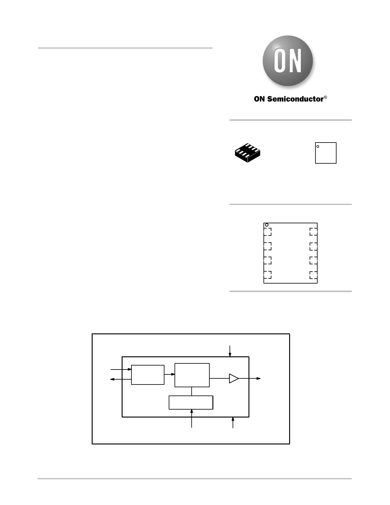
VDD
XIN/CLKIN
XOUT
Crystal
Oscillator
Digital
Frequency
Modulation
Analog Deviation
Control
ModOUT
SSEXTR
GND
Figure 1. Block Diagram
© Semiconductor Components Industries, LLC, 2012
August, 2012 − Rev. 0
1
Publication Order Number:
P3P8203A/D
1 page 
P3P8203A
0.060
0.055
0.050
0.045
0.040
0.035
0.0305 5.5 6 6.5 7
RESISTANCE (kW)
Figure 5. Deviation vs. SSEXTR (@ 27 MHz)
(NOTE: Parameter is guaranteed by design and characterization. Not tested in production.)
CL is the load capacitance for proper
XTAL operation
CL Y1
CL
VDDIN
R
C1
0.1 mF
C2
2.2 mF
1
XIN/C LKIN
8 VDD
ModOUT 5
2
XOUT
SSEXTR 7
3, 6
NC
P3P8203A
4 GND
Rs
ModOUT Cloc k
R1 Analog D eviation C ontrol
Note: Refer Pin Description table for Functionality details
Figure 6. Typical Application Circuit
Rs = Trace Impedance of PCB − Output Impedance of Device (Z0)
ORDERING INFORMATION
Ordering Code
Marking
Temperature
Package Type
Shipping†
P3P8203AMTTBG
GJ
0°C to +70°C
8−pin (2 mm x 2 mm) WDFN
3000 / Tape & Reel
(Pb−Free)
†For information on tape and reel specifications, including part orientation and tape sizes, please refer to our Tape and Reel Packaging
Specifications Brochure, BRD8011/D.
*A “microdot” placed at the end of last row of marking or just below the last row toward the center of package indicates Pb−Free.
http://onsemi.com
5
5 Page | ||
| Páginas | Total 6 Páginas | |
| PDF Descargar | [ Datasheet P3P8203A.PDF ] | |
Hoja de datos destacado
| Número de pieza | Descripción | Fabricantes |
| P3P8203A | General Purpose Peak EMI Reduction Device | ON Semiconductor |
| Número de pieza | Descripción | Fabricantes |
| SLA6805M | High Voltage 3 phase Motor Driver IC. |
Sanken |
| SDC1742 | 12- and 14-Bit Hybrid Synchro / Resolver-to-Digital Converters. |
Analog Devices |
|
DataSheet.es es una pagina web que funciona como un repositorio de manuales o hoja de datos de muchos de los productos más populares, |
| DataSheet.es | 2020 | Privacy Policy | Contacto | Buscar |