|
|
|
PDF PCA9306 Data sheet ( Hoja de datos )
| Número de pieza | PCA9306 | |
| Descripción | Dual Bidirectional I2C-bus and SMBus Voltage-Level Translator | |
| Fabricantes | ON Semiconductor | |
| Logotipo | ||
Hay una vista previa y un enlace de descarga de PCA9306 (archivo pdf) en la parte inferior de esta página. Total 12 Páginas | ||
|
No Preview Available !
PCA9306
Dual Bidirectional I2C-bus
and SMBus Voltage-Level
Translator
The PCA9306 is a dual bidirectional I2C−bus and SMBus
voltage−level translator with an enable (EN) input.
Features
• 2−bit Bidirectional Translator for SDA and SCL Lines in
Mixed−Mode I2C−Bus Applications
• Standard−Mode, Fast−Mode, and Fast−Mode Plus I2C−Bus and
SMBus Compatible
• Less Than 1.5 ns Maximum Propagation Delay to Accommodate
Standard−Mode and Fast−Mode I2C−Bus Devices and Multiple
Masters
• Allows Voltage Level Translation Between:
♦ 1.0 V Vref(1) and 1.8 V, 2.5 V, 3.3 V or 5 V Vbias(ref)(2)
♦ 1.2 V Vref(1) and 1.8 V, 2.5 V, 3.3 V or 5 V Vbias(ref)(2)
♦ 1.8 V Vref(1) and 3.3 V or 5 V Vbias(ref)(2)
♦ 2.5 V Vref(1) and 5 V Vbias(ref)(2)
♦ 3.3 V Vref(1) and 5 V Vbias(ref)(2)
• Provides Bidirectional Voltage Translation With No Direction Pin
• Low 3.5 W ON−State Connection Between Input and Output Ports
Provides Less Signal Distortion
• Open−Drain I2C−Bus I/O Ports (SCL1, SDA1, SCL2 and SDA2)
• 5 V Tolerant I2C−Bus I/O Ports to Support Mixed−Mode Signal
Operation
• High−Impedance SCL1, SDA1, SCL2 and SDA2 Pins for
EN = LOW
• Lock−Up Free Operation
• Flow Through Pinout for Ease of Printed−Circuit Board Trace
Routing
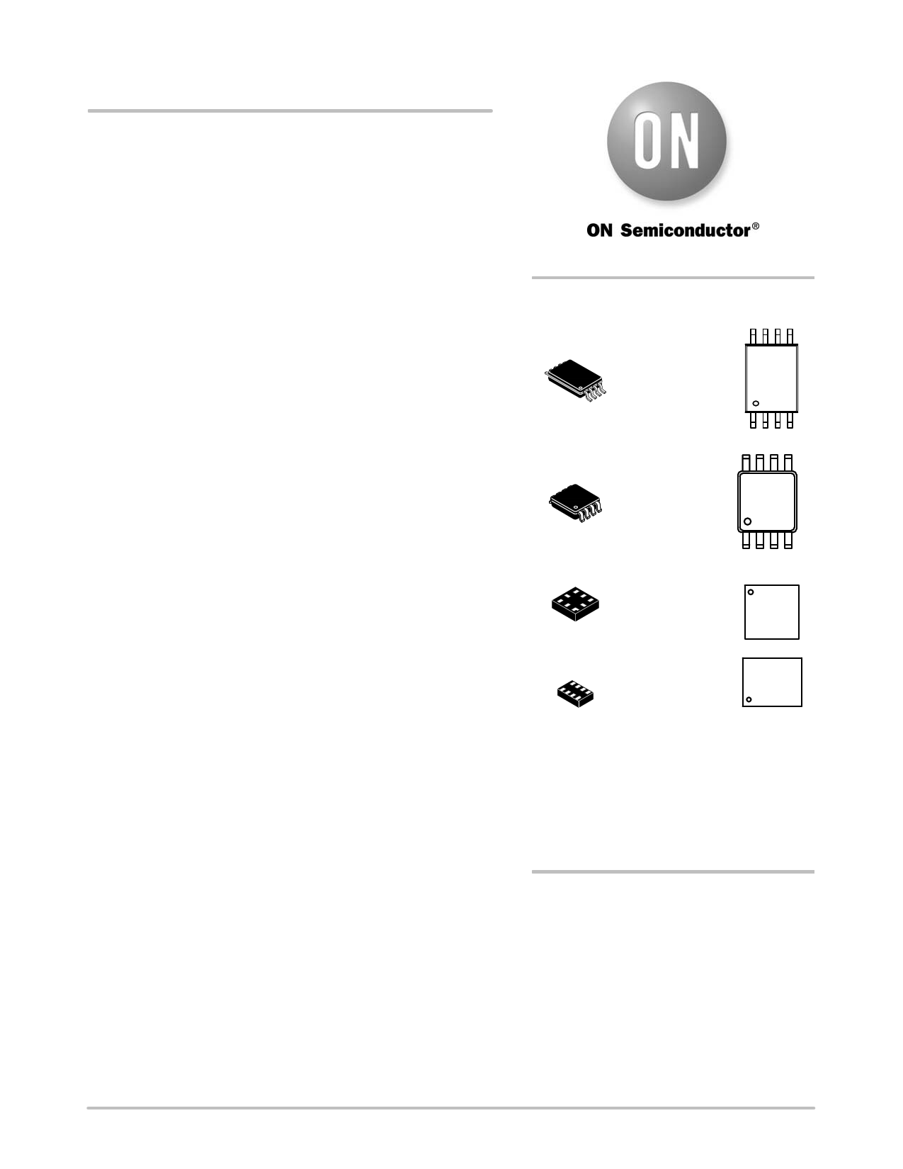
• Packages Offered:
♦ TSSOP−8, US8, UQFN8, UDFN8
• ESD Performance: 4000 V Human Body Model,
400 V Machine Model
• NLV Prefix for Automotive and Other Applications Requiring
Unique Site and Control Change Requirements; AEC−Q100
Qualified and PPAP Capable
• These are Pb−Free Devices
http://onsemi.com
TSSOP−8
DT SUFFIX
CASE 948AL
MARKING
DIAGRAMS
8
AAF
YWW-
AG
1
8
US8
US SUFFIX
CASE 493
AK MG
G
18
1
UQFN8
MU SUFFIX
CASE 523AN
1
AQ MG
UDFN8
PM
1.45 x 1.0
1
CASE 517BZ
AAF, AK, AQ, P = Specific Device Code
A = Assembly Location
Y = Year
WW = Work Week
M = Date Code
G = Pb−Free Package
ORDERING INFORMATION
See detailed ordering and shipping information in the package
dimensions section on page 6 of this data sheet.
© Semiconductor Components Industries, LLC, 2014
July, 2014 − Rev. 6
1
Publication Order Number:
PCA9306/D
1 page 
PCA9306
Table 5. DC ELECTRICAL CHARACTERISTICS
Symbol
VIK
IIH
Ci(EN)
Ci/O(off)
Parameter
Input Clamping Voltage
High−Level Input Current
EN Pin Input Capacitance
OFF−State I/O Pin Capacitance
SCLn, SDAn
Conditions
II = −18 mA; VI(EN) = 0 V
VI = 5 V; VI(EN) = 0 V
VI = 3 V or 0 V
VO = 3 V or 0 V; VI(EN) = 0 V
TA = −555C to +1255C
Typ
Min (Note 8) Max
−1.2
5
7.1
46
Unit
V
mA
pF
pF
Ci/O(on)
RON
ON−State I/O Pin Capacitance
SCLn, SDAn
ON−State Resistance(2)(3) SCLn, SDAn
VO = 3 V or 0 V;
VI(EN) = 3 V
VI = 0 V; IO = 64 mA
VI(EN) = 4.5 V
VI(EN) = 3 V
VI(EN) = 2.3 V
VI(EN) = 1.5 V
pF
9.3 12.5
W
2.4 5.0
3.0 6.0
3.8 8.0
9.0 20
VI = 2.4 V; IO = 15 mA
VI(EN) = 4.5 V
VI(EN) = 3 V
4.8 7.5
46 80
VI = 1.7 V; IO = 15 mA
VI(EN) = 2.3 V
40 80
Product parametric performance is indicated in the Electrical Characteristics for the listed test conditions, unless otherwise noted. Product
performance may not be indicated by the Electrical Characteristics if operated under different conditions.
8. All typical values are at TA = 25°C.
9. Measured by the voltage drop between the SCL1 and SCL2, or SDA1 and SDA2 terminals at the indicated current through the switch.
ON−state resistance is determined by the lowest voltage of the two terminals.
10. Guaranteed by design.
Table 6. AC ELECTRICAL CHARACTERISTICS (Translating Down) − Values Guaranteed by Design
Symbol
Parameter
Test Condition
Load
Condition
TA = −555C to +1255C
Min Max
SEE FIGURE 4 LOAD SWITCH AT S2 POSITION
tPLH Low−to−High Propagation De- VI(EN) = 3.3 V; VIH = 3.3 V; CL = 15 pF
lay, from (input) SCL2 or
SDA2 to (output) SCL1 or
VIL = 0 V; VM = 1.15 V
CL = 30 pF
SDA1
CL = 50 pF
tPHL High−to−Low Propagation De-
lay, from (input) SCL2 or
SDA2 to (output) SCL1 or
SDA1
CL = 15 pF
CL = 30 pF
CL = 50 pF
tPLH Low−to−High Propagation De- VI(EN) = 2.5 V; VIH = 2.5 V; CL = 15 pF
lay, from (input) SCL2 or
SDA2 to (output) SCL1 or
VIL = 0 V; VM = 0.75 V
CL = 30 pF
SDA1
CL = 50 pF
tPHL High−to−Low Propagation De-
lay, from (input) SCL2 or
SDA2 to (output) SCL1 or
SDA1
CL = 15 pF
CL = 30 pF
CL = 50 pF
0 0.6
0 1.2
0 2.0
0 0.75
0 1.5
0 2.0
0 0.6
0 1.2
0 2.0
0 0.75
0 1.5
0 2.5
Unit
ns
ns
http://onsemi.com
5
5 Page 
PCA9306
PACKAGE DIMENSIONS
UQFN8, 1.6x1.6, 0.5P
CASE 523AN
ISSUE O
D
PIN ONE
REFERENCE
2X
ÉÉÉÉ
0.10 C
2X
0.10 C
TOP VIEW
A
B
E
0.05 C
DETAIL B (A3)
0.05 C
SIDE VIEW
A1
8X L
3
8X
L3
5
e
EXPOSED Cu
ÇÉÇÉ
MOLD CMPD
A3
NOTES:
1. DIMENSIONING AND TOLERANCING PER
ASME Y14.5M, 1994.
2. CONTROLLING DIMENSION: MILLIMETERS.
3. DIMENSION b APPLIES TO PLATED TERMINAL
AND IS MEASURED BETWEEN 0.15 AND
0.30 mm FROM THE TERMINAL TIP.
A1
A
C
SEATING
PLANE
DETAIL B
MILLIMETERS
DIM MIN MAX
OPTIONAL
CONSTRUCTION
A 0.45 0.60
A1 0.00 0.05
A3 0.13 REF
b 0.15 0.25
L1 L3
D 1.60 BSC
E 1.60 BSC
e 0.50 BSC
L 0.35 0.45
L1 −−− 0.15
b
(0.10)
(0.15)
L3 0.25 0.35
DETAIL A
OPTIONAL
CONSTRUCTION
SOLDERING FOOTPRINT*
1.70 0.50
PITCH
1
DETAIL A
1
7
8 8X b
0.10 C A B
BOTTOM VIEW
0.05 C NOTE 3
0.35
7X 0.25
1.70
8X
0.53
DIMENSIONS: MILLIMETERS
*For additional information on our Pb−Free strategy and soldering
details, please download the ON Semiconductor Soldering and
Mounting Techniques Reference Manual, SOLDERRM/D.
http://onsemi.com
11
11 Page | ||
| Páginas | Total 12 Páginas | |
| PDF Descargar | [ Datasheet PCA9306.PDF ] | |
Hoja de datos destacado
| Número de pieza | Descripción | Fabricantes |
| PCA9306 | PCA9306 Dual Bidirectional I2C Bus and SMBus Voltage-Level Translator (Rev. L) | Texas Instruments |
| PCA9306 | Dual bidirectional I2C-bus and SMBus voltage-level translator | NXP Semiconductors |
| PCA9306 | Dual Bidirectional I2C-bus and SMBus Voltage-Level Translator | ON Semiconductor |
| PCA9306-Q1 | PCA9306-Q1 Dual Bidirectional I2C Bus and SMBus Voltage-Level Translator (Rev. A) | Texas Instruments |
| Número de pieza | Descripción | Fabricantes |
| SLA6805M | High Voltage 3 phase Motor Driver IC. |
Sanken |
| SDC1742 | 12- and 14-Bit Hybrid Synchro / Resolver-to-Digital Converters. |
Analog Devices |
|
DataSheet.es es una pagina web que funciona como un repositorio de manuales o hoja de datos de muchos de los productos más populares, |
| DataSheet.es | 2020 | Privacy Policy | Contacto | Buscar |