|
|
|
PDF NCV890430 Data sheet ( Hoja de datos )
| Número de pieza | NCV890430 | |
| Descripción | 0.6A 2MHz 100% Duty Cycle Step-Down Synchronous Regulator | |
| Fabricantes | ON Semiconductor | |
| Logotipo | ||
Hay una vista previa y un enlace de descarga de NCV890430 (archivo pdf) en la parte inferior de esta página. Total 9 Páginas | ||
|
No Preview Available !
NCV890430
Product Preview
0.6 A 2 MHz 100% Duty Cycle
Step‐Down Synchronous
Regulator for Automotive
The NCV890430 is a fixed-frequency Synchronous Buck regulator
intended for Automotive, battery-connected applications that operate
with up to a 45 V input supply. It is suitable for automotive systems
with high efficiency, low noise and Low Shutdown Current
requirements that also need to operate at low input voltage close to the
output voltage. A reset pin (with adjustable delay) simplifies
interfacing with a microcontroller. This part also features an enable
input that can either be connected to a low voltage (such as
a micro-controller output) or high voltage (such as the battery input),
and a synchronization input.
The NCV890430 also provides several protection features expected
in automotive power supply systems such as current limit, short circuit
protection, and thermal shutdown. In addition, the high switching
frequency produces low output voltage ripple even when using small
inductor values and all-ceramic input output filter capacitors −
forming a space-efficient switching regulator solution
Features
• Internal 500 mW P-channel and 250 mW N-channel Power Switches
• Capable of 100% Duty Cycle Operation
• VIN Operating Range 3.5 V to 37 V
• Withstands Load Dump to 45 V
• 2 MHz Free-running Switching Frequency
• Low Shutdown Current < 10 mA
• High Voltage Enable Pin
• Synchronization Input Pin
• DC Output Current of at Least 0.6 A
• Fixed Output Voltage (5 V, 3.3 V, 2.5 V Versions)
• ±2% Output Voltage Accuracy
• DFN Package with Wettable Flanks
(Pin Edge Plating per JEDEC MO220)
• NCV Prefix for Automotive Requiring Site and Control Changes
• These are Pb−Free Devices
Typical Applications
• Automotive Infotainment and Instrumentation
• Automotive Body Applications
• Linear Regulator Replacement
• Rear View Camera
www.onsemi.com
1
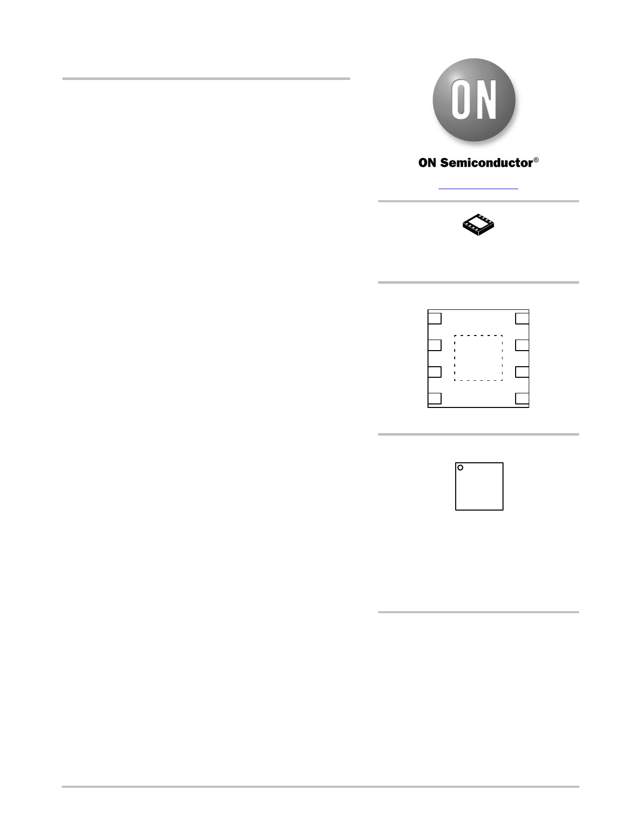
DFN8, 3x3, 0.65P
CASE 506CS
PIN CONNECTIONS
VIN 1
8 SW
RSTB
2
7 PGND
GND
3
6 SYNC
EN 4
5 VOUT
(DFN8 Top View)
MARKING DIAGRAM
1
XXXXXX
XXXXXX
ALYWG
G
XXXXX = Specific Device Code (TBD)
A = Assembly Location
L = Wafer Lot
Y = Year
W = Work Week
G = Pb−Free Package
(Note: Microdot may be in either location)
ORDERING INFORMATION
See detailed ordering, marking and shipping information on
page 8 of this data sheet.
This document contains information on some products that are still under development. ON
Semiconductor reserves the right to change or discontinue these products without notice.
© Semiconductor Components Industries, LLC, 2015
June, 2015 − Rev. P3
1
Publication Order Number:
NCV890430/D
1 page 
NCV890430
Table 3. ELECTRICAL CHARACTERISTICS (continued)
(VIN = 4.5 V to 28 V, EN = 5 V. Min/Max values are valid for the temperature range −40°C ≤ TJ ≤ 150°C unless noted otherwise,
and are guaranteed by test, design or statistical correlation.)
Parameter
Test Conditions
Symbol Min Typ Max Unit
HICCUP MODE
Hiccup Mode
Hiccup Mode 2 − SW Short to Battery
SYNCHRONIZATION
VSW = 0 V
VSW = 13.2 V
fSWHIC 24 32 40 kHz
fSWHICLS
24
32
40 kHz
SYNC Input Resistance to Ground
SYNC Input High Threshold Voltage
SYNC Input Low Threshold Voltage
SYNC High Pulse Width
SYNC Low Pulse Width
External SYNC Frequency
Master Reassertion Time
VSYNC = 5.0 V
RH(SYNC)
50
200 kW
VHSYNC
2.0
V
VLSYNC
0.8 V
VSYNC > max VHSYNC
tHSYNC
40
ns
VSYNC < min VLSYNC
tLSYNC
40
ns
fSYNC
1.8
2.5 MHz
Time from Last Rising SYNC Edge
tI(SYNC)
650
ns
to First Un-synchronized Turn-on.
RESET
Reset Threshold
Reset Hysteresis (Ratio of VOUT)
Leakage Current into RSTB Pin
VOUT Decreasing
VOUT Increasing
KRES_LO
KRES_HI
KRES_HYS
91
91.5
0.5
93
95 %
97
%
1.0 mA
Noise-Filtering Delay
From VOUT < VRESET to RSTB Pin
Going Low
tRES_FILT
10
25 ms
Reset Delay Time
Reset Delay Modes
IRSTB = 1.1 mA
IRSTB = 500 mA
IRSTB = 100 mA
Power Good Mode (No Delay)
Delay Mode
tRESET 1.0 ms
4.0 5.0 6.0 ms
19 24 29 ms
1000
mA
600
Reset Output Low Level
ENABLE
IRSTB = 1.2 mA
VRESL
0.4 V
Logic Low Threshold Voltage
Logic High Threshold Voltage
EN Pin Input Current
THERMAL SHUTDOWN
VENlow
VENhigh
IENbias
2.0
8.0
0.8 V
V
30 mA
Thermal Shutdown Activation Temperature
(Note 2)
TSD 155
190 °C
Hysteresis (Note 2)
THYS
5.0
20 °C
Product parametric performance is indicated in the Electrical Characteristics for the listed test conditions, unless otherwise noted. Product
performance may not be indicated by the Electrical Characteristics if operated under different conditions.
2. Not tested in production. Limits are guaranteed by design.
www.onsemi.com
5
5 Page | ||
| Páginas | Total 9 Páginas | |
| PDF Descargar | [ Datasheet NCV890430.PDF ] | |
Hoja de datos destacado
| Número de pieza | Descripción | Fabricantes |
| NCV890430 | 0.6A 2MHz 100% Duty Cycle Step-Down Synchronous Regulator | ON Semiconductor |
| Número de pieza | Descripción | Fabricantes |
| SLA6805M | High Voltage 3 phase Motor Driver IC. |
Sanken |
| SDC1742 | 12- and 14-Bit Hybrid Synchro / Resolver-to-Digital Converters. |
Analog Devices |
|
DataSheet.es es una pagina web que funciona como un repositorio de manuales o hoja de datos de muchos de los productos más populares, |
| DataSheet.es | 2020 | Privacy Policy | Contacto | Buscar |