|
|
|
PDF AP65353 Data sheet ( Hoja de datos )
| Número de pieza | AP65353 | |
| Descripción | 50kHz ADAPTIVE COT STEP-DOWN CONVERTER | |
| Fabricantes | Diodes | |
| Logotipo | ||
Hay una vista previa y un enlace de descarga de AP65353 (archivo pdf) en la parte inferior de esta página. Total 15 Páginas | ||
|
No Preview Available !
AP65353
3A, 18V, 650kHz ADAPTIVE COT STEP-DOWN CONVERTER
Description
The AP65353 is an adaptive constant on-time mode synchronous
buck converter providing high efficiency, excellent transient response
and high DC output accuracy for low-voltage regulation in digital
TV and monitor.
The constant-on-time control scheme handles wide input/output
voltage ratios and provides low external component count. The
internal proprietary circuit enables the device to adopt both low
equivalent series resistance (ESR) output capacitors, such as
SP-CAP or POSCAP and ultra-low ESR ceramic capacitors.
The adaptive on-time control supports seamless transition between
continuous conduction mode (CCM) at higher load conditions and
discontinuous conduction mode (DCM) at lighter load conditions.
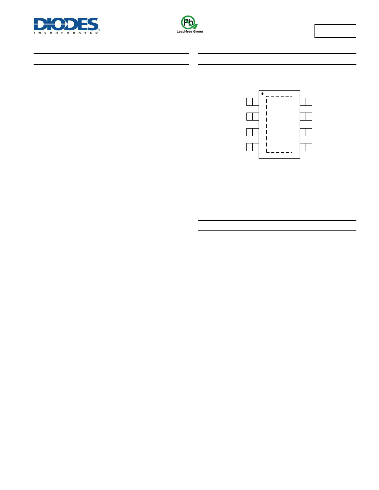
Pin Assignments
( Top View )
EN 1
FB 2
VREG5 3
SS 4
Exposed
Pad
9
SO-8EP
8 VIN
7 BS
6 SW
5 PGND
DCM allows AP65353 to maintain high efficiency at light load
conditions. The AP65353 also features programmable soft-start,
UVLO, OTP, OVP and OCP to protect the circuit.
This IC is available in SO-8EP package.
Features
Fixed Frequency Emulated Constant On-Time Control
Good Stability Independent of the Output Capacitor ESR
Fast Load Transient Response
Synchronous Rectification: 90mΩ Internal High-side Switch and
57mΩ Internal Low-Side Switch
Wide Input Voltage Range: 4.5V to 18V
Output Voltage Range: 0.76V to 6V
3A Continuous Output Current
650kHz Switching Frequency
Built-in Over Current Limit
Built-in Over Voltage Protection
Built-in Thermal Shutdown Protection
Programmable Soft-Start
Pre-biased Start-Up
Totally Lead-Free & Fully RoHS Compliant (Notes 1 & 2)
Halogen and Antimony Free. “Green” Device (Note 3)
Notes:
1. No purposely added lead. Fully EU Directive 2002/95/EC (RoHS) & 2011/65/EU (RoHS 2) compliant.
2. See http://www.diodes.com/quality/lead_free.html for more information about Diodes Incorporated’s definitions of Halogen- and Antimony-free, "Green"
and Lead-free.
3. Halogen- and Antimony-free "Green” products are defined as those which contain <900ppm bromine, <900ppm chlorine (<1500ppm total Br + Cl) and
<1000ppm antimony compounds.
AP65353
Document number: DS37925 Rev. 1- 2
1 of 15
www.diodes.com
June 2015
© Diodes Incorporated
1 page 
AP65353
Electrical Characteristics (@TA = +25°C, VIN = 12V, unless otherwise specified.)
Parameter
SUPPLY VOLTAGE (VIN PIN)
Input Voltage
Quiescent Current
Shutdown Supply Current
UNDER VOLTAGE LOCKOUT
UVLO Threshold
UVLO Hysteresis
ENABLE (EN PIN)
EN High-level Input Voltage
EN Low-level Input Voltage
VOLTAGE REFERENCE (FB PIN)
Feedback Voltage
Feedback Bias Current
VREG5 OUTPUT
VREG5 Output Voltage
Source Current Capability
Load Regulation
Line Regulation
MOSFET
High-side Switch On-resistance
Low-side Switch On-resistance
CURRENT LIMIT
High Level Current Limit
ON-TIME TIMER
On Time
Minimum Off Time
THERMAL SHUTDOWN
Thermal Shutdown
Thermal Shutdown Hysteresis
SOFT START (SS PIN)
Soft-Start Source Current
Soft-Start Discharge Current
OVERVOLTAGE PROTECTION
OVP Trip Threshold
Symbol
Conditions
VIN
IQ
ISHDN
VFB = 0.85V
VEN = 0V
—
VUVLO
VHYS
VENH
VENL
VIN Rising Test VREG5 Voltage
VIN Falling Test VREG5 Voltage
—
—
VFB VOUT = 1.05V
IFB VFB = 0.8V
VVREG5
—
—
—
RDSONH
RDSONL
6.0V < VIN < 18V 0 < IVREG5 < 5mA
VIN = 6V, VVREG5 = 4V
0 < IVREG5 < 5mA
6.0V < VIN < 18V IVREG5 = 5mA
—
—
ILIM-H
L = 1.5μH
tON
tOFF-MIN
TOTSD
THYS
VIN = 12V, VOUT = 1.05V
VFB = 0.7V
—
—
ISS-SOURCE
ISS-DISCHARGE
VSS = 1.0V
VSS = 0.5V
—
—
Min
4.5
—
—
3.6
0.16
1.25
—
0.753
-0.1
4.8
—
—
—
—
—
3.9
—
—
—
—
4.2
0.1
115
Typ
—
0.6
1
3.85
0.35
—
—
0.765
0
5.1
100
—
—
0.090
0.057
4.5
150
260
150
25
6.0
0.2
120
Max
18
0.75
10
4.1
0.47
18
0.85
0.777
0.1
5.4
—
100
20
—
—
5.5
—
310
—
—
7.8
—
125
Unit
V
mA
μA
V
V
V
V
V
μA
V
mA
mV
mV
Ω
Ω
A
ns
ns
°C
°C
μA
mA
%
AP65353
Document number: DS37925 Rev. 1- 2
5 of 15
www.diodes.com
June 2015
© Diodes Incorporated
5 Page 
Application Information (cont.)
Figure 5 Feedback Divider Network
AP65353
Output Voltage (V)
1
1.05
1.2
1.5
1.8
2.5
3.3
5
R1 (kΩ)
6.81
8.25
12.7
21.5
30.1
49.9
73.2
124
R2 (kΩ)
22.1
22.1
22.1
22.1
22.1
22.1
22.1
22.1
Table 1 Resistor Selection for Common Output
Voltages
Inductor
Calculating the inductor value is a critical factor in designing a buck converter. For most designs, the following equation can be used to calculate
the inductor value:
L
VOUT (VIN
VIN ΔIL
VOUT
fSW
)
Where ΔIL is the inductor ripple current and fSW is the buck converter switching frequency.
Choose the inductor ripple current to be 30% of the maximum load current. The maximum inductor peak current is calculated from:
IL(MAX)
ILOAD
ΔIL
2
Peak current determines the required saturation current rating, which influences the size of the inductor. Saturating the inductor decreases the
converter efficiency while increasing the temperatures of the inductor and the internal MOSFETs. Hence choosing an inductor with appropriate
saturation current rating is important.
A 1µH to 3.3µH inductor with a DC current rating of at least 25% percent higher than the maximum load current is recommended for most
applications. For highest efficiency, the inductor’s DC resistance should be less than 100mΩ. Use a larger inductance for improved efficiency
under light load conditions.
The phase boost can be achieved by adding an additional feed forward capacitor (C7) in parallel with R1.
Output Voltage (V)
1
1.05
1.2
1.5
1.8
2.5
3.3
5
C7(pF)
—
—
—
—
5-22
5-22
5-22
5-22
L1(µH)
1.0-1.5
1.0-1.5
1.0-1.5
1.5
1.5
2.2
2.2
3.3
Table 2 Recommended Component Selection
C8+C9(µF)
22-68
22-68
22-68
22-68
22-68
22-68
22-68
22-68
Input Capacitor
The input capacitor reduces the surge current drawn from the input supply and the switching noise from the device. The input capacitor has to
sustain the ripple current produced during the on time on the upper MOSFET. It must have a low ESR to minimize the losses.
The RMS current rating of the input capacitor is a critical parameter that must be higher than the RMS input current. As a rule of thumb, select an
input capacitor which has RMs rating greater than half of the maximum load current.
Due to large dI/dt through the input capacitors, electrolytic or ceramics should be used. If a tantalum must be used it must be surge protected,
otherwise, capacitor failure could occur. For most applications greater than 10µF, ceramic capacitor is sufficient.
AP65353
Document number: DS37925 Rev. 1- 2
11 of 15
www.diodes.com
June 2015
© Diodes Incorporated
11 Page | ||
| Páginas | Total 15 Páginas | |
| PDF Descargar | [ Datasheet AP65353.PDF ] | |
Hoja de datos destacado
| Número de pieza | Descripción | Fabricantes |
| AP65352 | 650kHz ADAPTIVE COT STEP-DOWN CONVERTER | Diodes |
| AP65353 | 50kHz ADAPTIVE COT STEP-DOWN CONVERTER | Diodes |
| AP65355 | 650kHz ADAPTIVE COT STEP-DOWN CONVERTER | Diodes |
| Número de pieza | Descripción | Fabricantes |
| SLA6805M | High Voltage 3 phase Motor Driver IC. |
Sanken |
| SDC1742 | 12- and 14-Bit Hybrid Synchro / Resolver-to-Digital Converters. |
Analog Devices |
|
DataSheet.es es una pagina web que funciona como un repositorio de manuales o hoja de datos de muchos de los productos más populares, |
| DataSheet.es | 2020 | Privacy Policy | Contacto | Buscar |