|
|
|
PDF ICS8745BI-21 Data sheet ( Hoja de datos )
| Número de pieza | ICS8745BI-21 | |
| Descripción | 1:1 Differential-to-LVDS Zero Delay Clock Generator | |
| Fabricantes | Integrated Device Technology | |
| Logotipo | ||
Hay una vista previa y un enlace de descarga de ICS8745BI-21 (archivo pdf) en la parte inferior de esta página. Total 21 Páginas | ||
|
No Preview Available !
1:1 Differential-to-LVDS Zero Delay
Clock Generator
ICS8745BI-21
DATA SHEET
General Description
Features
The ICS8745BI-21 is a highly versatile 1:1 LVDS Clock Generator.
The ICS8745BI-21 has a fully integrated PLL and can be configured
as a zero delay buffer, multiplier or divider, and has an output
frequency range of 31.25MHz to 700MHz. The Reference Divider,
Feedback Divider and Output Divider are each programmable,
thereby allowing for the following output-to-input frequency ratios:
8:1, 4:1, 2:1, 1:1, 1:2, 1:4, 1:8. The external feedback allows the
device to achieve “zero delay” between the input clock and the
output clock. The PLL_SEL pin can be used to bypass the PLL for
system test and debug purposes. In bypass mode, the reference
clock is routed around the PLL and into the internal output dividers.
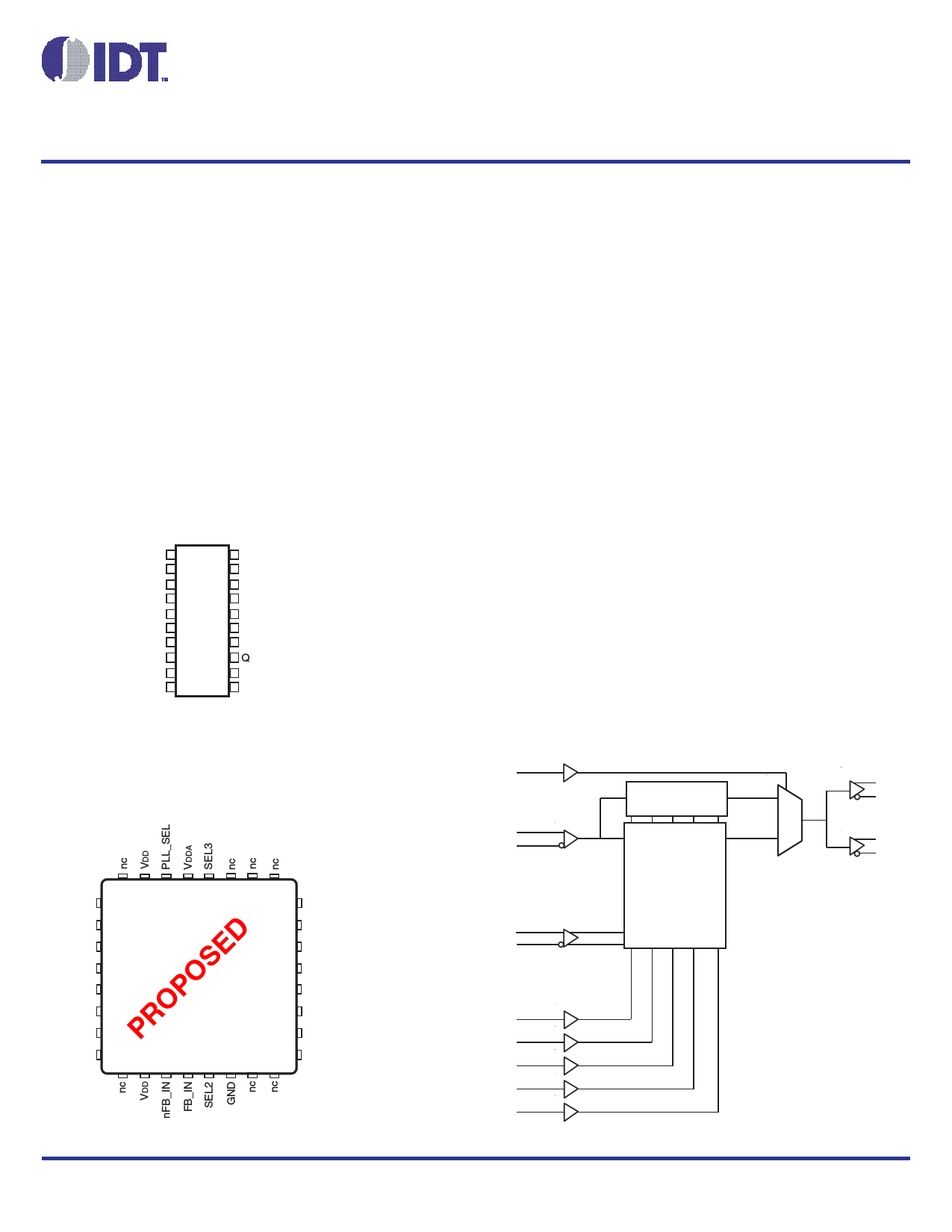
Pin Assignments
CLK
nCLK
MR
nFB_IN
FB_IN
SEL2
VDDO
nQFB
QFB
GND
1
2
3
4
5
6
7
8
9
10
20 SEL1
19 SEL0
18 VDD
17 PLL_SEL
16 VDDA
15 SEL3
14 GND
13 Q
12 nQ
11 VDDO
ICS8745BI-21
• One differential LVDS output designed to meet
or exceed the requirements of ANSI TIA/EIA-644
One differential feedback output pair
• Differential CLK, nCLK input pair
• CLKx, nCLKx pair can accept the following differential
input levels: LVPECL, LVDS, LVHSTL, HCSL, SSTL
• Output frequency range: 31.25MHz to 700MHz
• Input frequency range: 31.25MHz to 700MHz
• VCO range: 250MHz to 700MHz
• External feedback for “zero delay” clock regeneration
with configurable frequencies
• Programmable dividers allow for the following output-to-input
frequency ratios: 8:1, 4:1, 2:1, 1:1, 1:2, 1:4, 1:8
• Cycle-to-cycle jitter: 30ps (maximum)
• Output skew: 40ps (maximum)
• Static phase offset: 25ps ± 125ps
• Full 3.3V supply voltage
• -40°C to 85°C ambient operating temperature
• Available in both standard (RoHS 5) and lead-free (RoHS 6)
packages
20-Lead SOIC
7.5mm x 12.8mm x 2.3mm package body
M Package
Top View
Block Diagram
PLL_SEL Pullup
÷1, ÷2, ÷4, ÷8,
÷16, ÷32,÷64
0
Q
nQ
CLK Pulldown
nCLK Pullup
1 QFB
nQFB
32 31 30 29 28 27 26 25
SEL0 1
24 GND
SEL1
nc
nc
CLK
nCLK
nc
2 ICS8745BI-21 23
3 32 Lead VFQFN 22
4 5mm x 5mm x 0.925mm 21
5 package body 20
6 K Package 19
7 Top View 18
Q
nQ
VDDO
GND
QFB
nQFB
MR 8
17 VDDO
9 10 11 12 13 14 15 16
FB_IN Pulldown
nFB_IN Pullup
SEL0 Pulldown
SEL1 Pulldown
SEL2 Pulldown
SEL3 Pulldown
MR Pulldown
PLL
8:1, 4:1, 2:1, 1:1,
1:2, 1:4, 1:8
ICS8745BMI-21 REVISION D JULY 28, 2010
1
©2010 Integrated Device Technology, Inc.
1 page 
ICS8745BI-21 Data Sheet
1:1 DIFFERENTIAL-TO-LVDS ZERO DELAY CLOCK GENERATOR
Absolute Maximum Ratings
NOTE: Stresses beyond those listed under Absolute Maximum Ratings may cause permanent damage to the device.
These ratings are stress specifications only. Functional operation of product at these conditions or any conditions beyond
those listed in the DC Characteristics or AC Characteristics is not implied. Exposure to absolute maximum rating conditions for
extended periods may affect product reliability.
Item
Supply Voltage, VDD
Inputs, VI
Outputs, IO
Continuous Current
Surge Current
Package Thermal Impedance, θJA
20 Lead SOIC package
32 Lead VFQFN package
Storage Temperature, TSTG
Rating
4.6V
-0.5V to VDD + 0.5V
10mA
15mA
46.2°C/W (0 lfpm)
37°C/W (0 mps)
-65°C to 150°C
DC Electrical Characteristics
Table 4A. LVDS Power Supply DC Characteristics, VDD = VDDO = 3.3V ± 5%, TA = -40°C to 85°C
Symbol Parameter
Test Conditions
Minimum Typical
VDD
VDDA
VDDO
IDD
IDDA
IDDO
Core Supply Voltage
Analog Supply Voltage
Output Supply Voltage
Power Supply Current
Analog Supply Current
Output Supply Current
3.135
3.135
3.135
3.3
3.3
3.3
Maximum
3.465
3.465
3.465
128
18
62
Units
V
V
V
mA
mA
mA
Table 4B. LVCMOS/LVTTL DC Characteristics, VDD = VDDO = 3.3V ± 5%, TA = -40°C to 85°C
Symbol Parameter
Test Conditions
Minimum Typical
VIH Input High Voltage
VIL Input Low Voltage
SEL[0:3], MR
IIH
Input High Current
PLL_SEL
SEL[0:3], MR
IIL Input Low Current
PLL_SEL
VDD = VIN = 3.465V
VDD = VIN = 3.465V
VDD = 3.465V, VIN = 0V
VDD = 3.465V, VIN = 0V
2
-0.3
-5
-150
Maximum
VDD + 0.3
0.8
150
5
Units
V
V
µA
µA
µA
µA
ICS8745BMI-21 REVISION D JULY 28, 2010
5
©2010 Integrated Device Technology, Inc.
5 Page 
ICS8745BI-21 Data Sheet
1:1 DIFFERENTIAL-TO-LVDS ZERO DELAY CLOCK GENERATOR
Differential Clock Input Interface
The CLK /nCLK accepts LVDS, LVPECL, LVHSTL, SSTL, HCSL and
other differential signals. Both differential signals must meet the VPP
and VCMR input requirements. Figures 3A to 3F show interface
examples for the CLK/nCLK input driven by the most common driver
types. The input interfaces suggested here are examples only.
Please consult with the vendor of the driver component to confirm the
driver termination requirements. For example, in Figure 3A, the input
termination applies for IDT open emitter LVHSTL drivers. If you are
using an LVHSTL driver from another vendor, use their termination
recommendation.
1.8V
Zo = 50Ω
Zo = 50Ω
LVHSTL
IDT
LVHSTL Driver
3.3V
CLK
R1 R2
50Ω 50Ω
nCLK
Differential
Input
3A. CLK/nCLK Input Driven by an
IDT Open Emitter LVHSTL Driver
3.3V
LVPECL
Zo = 50Ω
Zo = 50Ω
3.3V
R3
125Ω
R4
125Ω
3.3V
CLK
nCLK
Differential
R1 R2
84Ω 84Ω
Input
3.3V
LVPECL
Zo = 50Ω
Zo = 50Ω
3.3V
CLK
R1 R2
50Ω 50Ω
nCLK
Differential
Input
R2
50Ω
Figure 3B. CLK/nCLK Input Driven by a
3.3V LVPECL Driver
3.3V
LVDS
Zo = 50Ω
Zo = 50Ω
3.3V
R1
100Ω
CLK
nCLK
Receiver
Figure 3C. CLK/nCLK Input Driven by a
3.3V LVPECL Driver
3.3V
3.3V
*R3 33Ω
Zo = 50Ω
Zo = 50Ω
HCSL
*R4 33Ω
*Optional – R3 and R4 can be 0Ω
R1
50Ω
CLK
nCLK
R2
50Ω
Differential
Input
Figure 3E. CLK/nCLK Input Driven by a
3.3V HCSL Driver
ICS8745BMI-21 REVISION D JULY 28, 2010
Figure 3D. CLK/nCLK Input Driven by a
3.3V LVDS Driver
2.5V
SSTL
Zo = 60Ω
Zo = 60Ω
2.5V
R3
120Ω
R4
120Ω
3.3V
CLK
R1
120Ω
R2
120Ω
nCLK
Differential
Input
Figure 3F. CLK/nCLK Input Driven by a
2.5V SSTL Driver
11 ©2010 Integrated Device Technology, Inc.
11 Page | ||
| Páginas | Total 21 Páginas | |
| PDF Descargar | [ Datasheet ICS8745BI-21.PDF ] | |
Hoja de datos destacado
| Número de pieza | Descripción | Fabricantes |
| ICS8745BI-21 | 1:1 Differential-to-LVDS Zero Delay Clock Generator | Integrated Device Technology |
| Número de pieza | Descripción | Fabricantes |
| SLA6805M | High Voltage 3 phase Motor Driver IC. |
Sanken |
| SDC1742 | 12- and 14-Bit Hybrid Synchro / Resolver-to-Digital Converters. |
Analog Devices |
|
DataSheet.es es una pagina web que funciona como un repositorio de manuales o hoja de datos de muchos de los productos más populares, |
| DataSheet.es | 2020 | Privacy Policy | Contacto | Buscar |