|
|
|
PDF CMX8341 Data sheet ( Hoja de datos )
| Número de pieza | CMX8341 | |
| Descripción | Digital PMR (dPMR) Baseband Processor | |
| Fabricantes | Consumer Microcircuits Limited | |
| Logotipo | ||
Hay una vista previa y un enlace de descarga de CMX8341 (archivo pdf) en la parte inferior de esta página. Total 30 Páginas | ||
|
No Preview Available !
CML Microcircuits
COMMUNICATION SEMICONDUCTORS
CMX8341
Digital PMR (dPMR)
Baseband Processor
D/8341/7 January 2014
DATASHEET
Advance Information
8341 FI-1.x Dual-mode Analogue PMR and Digital PMR (dPMR) Baseband
Processing
Features
Digital PMR (dPMR) Baseband Processor
o dPMR (ETSI TS 102 490) Compliant
o Air Interface Physical Layer (Layer 1)
o Air Interface Data Link layer (Layer 2)
o 4FSK Modem
Soft-decision Decoding
AFSD (Automatic Frame Sync Detection)
RALCWI Vocoder
o Fully Embedded Implementation
o No Licensing or Royalty payments
o 3600bps Over Air Data Rate
(2400bps Voice plus 1200bps Robust FEC)
o 4-bit Viterbi Soft-decision Decoding
Analogue PMR (Legacy mode)
o Full Audio Band Processing
o Sub-audio Filtering
o CTCSS and DCS
o 12.5 and 25kHz Channel Filters
Built on FirmASIC™ Technology
o Function Image™ 8341FI-1.x Required
o Serial Memory or Host Loading
o Integration Roadmap
Auxiliary functions
o 2 System Clock Outputs
o Tx PA Ramp DAC
o 3 DACs, 4 inputs Multiplexed to 2 ADCs
o GPIO
o Tx Enable and Rx Enable Outputs
Half-duplex Operation
Input from RF Discriminator
2-point Modulation Drivers
Audio Output with Volume Control
Microphone Input
Low Power Operation
LQFP packaging
Applications
Low Cost Digital PMR Radios
Low Cost Digital PMR with Legacy Analogue
PMR Mode
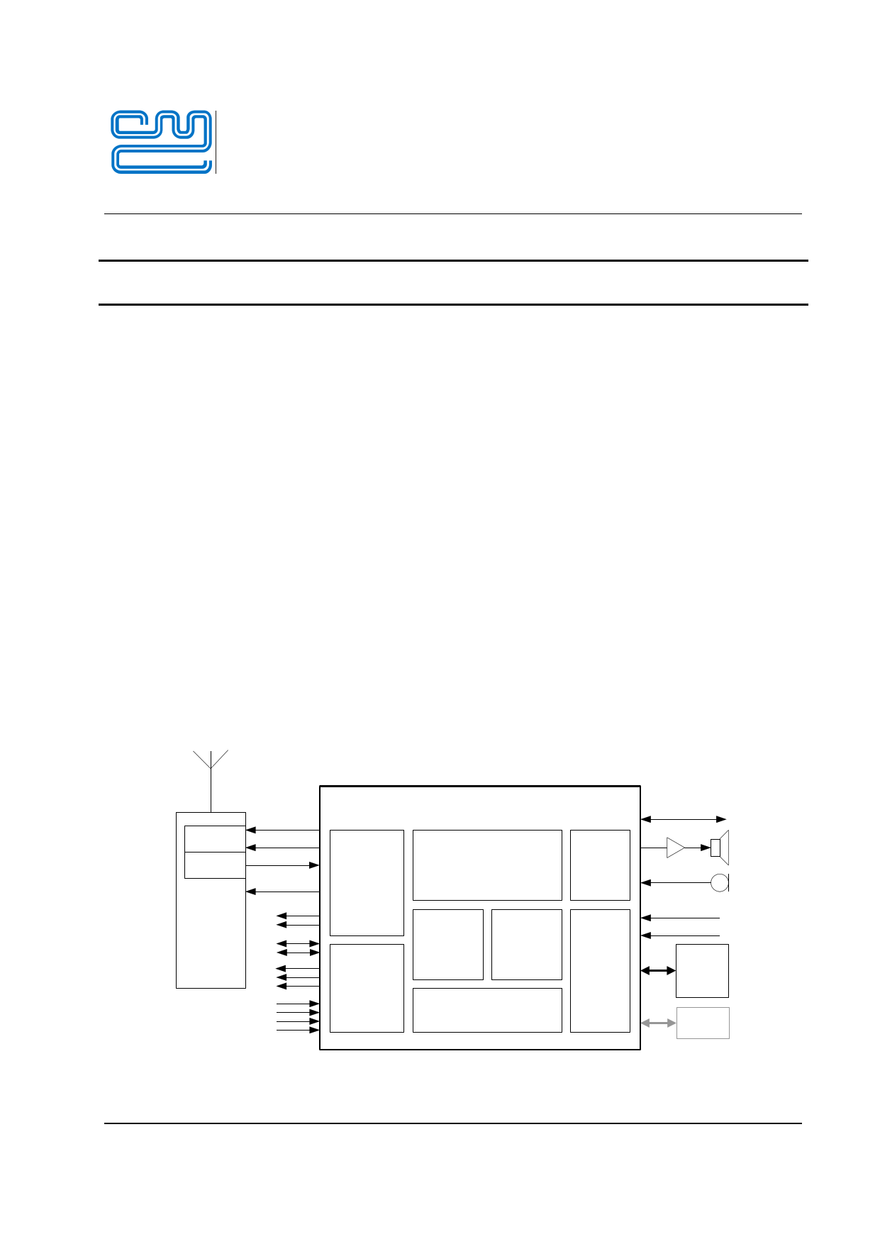
Modulator
Discriminator
RF
Section
PA Ramp
PLL
Clocks
GPIO
DACs
Mux
ADC
CMX8341 dPMR Baseband Processor
External Sub-audio
RF
Interface
Digital PMR Air Interface:
Physical, Data Link and
Control Layer Support
Audio
Interface
Auxiliary
Operations
Data
Modem
Vocoder
Analogue PMR:
Core Functionality
System
Control
External Ref. Clock
Power Supplies
C-BUS
µC
Interface
Serial
Memory
(Optional)
2014 CML Microsystems Plc
1 page 
Digital PMR (dPMR) Baseband Processor
CMX8341
Table
Page
Table 1 Definition of Power Supply and Reference Voltages........................................... 12
Table 2 Recommended Component Values .................................................................... 14
Table 3 dPMR Frame Format - Call set-up, no ACK ....................................................... 23
Table 4 dPMR Frame Format - Call set-up with ACK ...................................................... 23
Table 5 DCS codes and values........................................................................................ 28
Table 6 CTCSS codes and values ................................................................................... 30
Table 7 BOOTEN Pin States............................................................................................ 33
Table 8 Modem Mode Selection ...................................................................................... 39
Table 9 Modem Control Selection.................................................................................... 39
Table 10 C-BUS Data Registers ...................................................................................... 44
Table 11 C-BUS Registers ............................................................................................... 58
Figure
Page
Figure 1 Block Diagram...................................................................................................... 8
Figure 2 Recommended External Components ............................................................... 13
Figure 3 Serial Memory Connections ............................................................................... 15
Figure 4 Other Connections ............................................................................................. 15
Figure 5 Tx Routing – Autonomous mode ....................................................................... 16
Figure 6 Rx Routing – Autonomous mode ....................................................................... 16
Figure 7 4FSK PRBS Waveform - Modulation................................................................. 20
Figure 8 4FSK PRBS Waveform - Spectrum ................................................................... 20
Figure 9 dPMR Modulation Characteristics...................................................................... 21
Figure 10 Internal Data Processing Blocks ...................................................................... 22
Figure 11 FS Detection .................................................................................................... 24
Figure 12 Rx Audio Response ......................................................................................... 27
Figure 13 Tx Audio Response.......................................................................................... 27
Figure 14 CTCSS and DCS filters.................................................................................... 28
Figure 15 C-BUS Transactions ........................................................................................ 32
Figure 16 FI Loading from Host ....................................................................................... 35
Figure 17 FI Loading from an external Serial Memory..................................................... 36
Figure 18 Tx Data Flow .................................................................................................... 41
Figure 19 Rx Data Flow.................................................................................................... 43
Figure 20 AuxADC IRQ Operation ................................................................................... 52
Figure 21 Digital Clock Generation Schemes .................................................................. 53
Figure 22 Tx Level Adjustments (Analogue) .................................................................... 55
Figure 23 Tx Levels (Digital) ............................................................................................ 55
Figure 24 Rx Level Adjustments (Analogue).................................................................... 56
Figure 25 Rx Level Adjustments (Digital) ......................................................................... 56
Figure 26 Tx Modulation Spectra - 4800bps .................................................................... 57
Figure 27 C-BUS Timing .................................................................................................. 68
Figure 28 L8 Mechanical Outline: Order as part no. CMX8341L8 .................................. 69
It is always recommended that you check for the latest product datasheet version from the
Datasheets page of the CML website: [www.cmlmicro.com].
2014 CML Microsystems Plc
5
D/8341/7
5 Page 
Digital PMR (dPMR) Baseband Processor
CMX8341
CMX8341L8
Pin
Description
Pin No.
Name
Type
Power Supplies and No Connections
32, 47, 57, 60,
66, 70, 72, 74, 94
DVDD
PWR
DVDD: Digital +3.3V supply rail. This pin should be
decoupled to DVSS by capacitors mounted close to the
device pins.
53, 95
VDEC
PWR
VDEC: Internally generated 2.5V supply voltage. Must be
decoupled to DVSS by capacitors mounted close to the
device pins. No other connections allowed.
31, 96
4, 6, 44, 49, 51,
52, 63, 65, 68,
85, 89, 100
CVDD
DVSS
PWR
Digital core +1.8V supply rail. This pin should be decoupled
to DVSS by capacitors mounted close to the device pins.
PWR DVSS: Negative Digital Supply
5, 9, 17, 19, 21,
40
AVSS
PWR AVSS: Negative Analogue Supply
2, 14, 26,35
AVDD
PWR
AVDD: Analogue +3.3V supply rail. Levels and thresholds
within the device are proportional to this voltage. This pin
should be decoupled to AVSS by capacitors mounted close
to the device pins.
Internally generated bias voltage of about AVDD/2, except
when the device is in ‘Powersave’ mode when voltage on
8
VBIAS
PWR VBIAS pin will discharge to AVSS. Must be decoupled to
AVSS by a capacitor mounted close to the device pins. No
other connections allowed. Do not connect to BIAS pin.
Internally generated bias voltage of about AVDD/2, except
when the device is in ‘Powersave’ mode when voltage on
27
BIAS
PWR BIAS pin will discharge to AVSS. Must be decoupled to AVSS
by a capacitor mounted close to the device pins No other
connections allowed. Do not connect to VBIAS pin.
38, 39, 43, 45,
46, 58, 67, 75,
77, 79, 80, 82, 99
n/c
NC Do not make any connection to this pin
Notes:
IP =
IP + PU =
IP + PD =
OP =
BI =
T/S =
PWR =
NC =
Input
Input with internal pullup resistor
Input with internal pulldown resistor
Output
Bidirectional Digital Signal
3-state Digital Output
Power Supply
No Connection
2014 CML Microsystems Plc
11
D/8341/7
11 Page | ||
| Páginas | Total 30 Páginas | |
| PDF Descargar | [ Datasheet CMX8341.PDF ] | |
Hoja de datos destacado
| Número de pieza | Descripción | Fabricantes |
| CMX8341 | Digital PMR (dPMR) Baseband Processor | Consumer Microcircuits Limited |
| Número de pieza | Descripción | Fabricantes |
| SLA6805M | High Voltage 3 phase Motor Driver IC. |
Sanken |
| SDC1742 | 12- and 14-Bit Hybrid Synchro / Resolver-to-Digital Converters. |
Analog Devices |
|
DataSheet.es es una pagina web que funciona como un repositorio de manuales o hoja de datos de muchos de los productos más populares, |
| DataSheet.es | 2020 | Privacy Policy | Contacto | Buscar |