|
|
|
PDF L8565 Data sheet ( Hoja de datos )
| Número de pieza | L8565 | |
| Descripción | HIGH PERFORMANCE POWER FACTOR CORRECTION CONTROLLER | |
| Fabricantes | Unisonic Technologies | |
| Logotipo | ||
Hay una vista previa y un enlace de descarga de L8565 (archivo pdf) en la parte inferior de esta página. Total 13 Páginas | ||
|
No Preview Available !
UNISONIC TECHNOLOGIES CO., LTD
L8565
Preliminary
LINEAR INTEGRATED CIRCUIT
HIGH PERFORMANCE POWER
FACTOR CORRECTION
CONTROLLER IN CONTINUOUS
CONDUCTION MODE
DESCRIPTION
The UTC L8565 is a wide input range controller integrated circuit for
active power factor correction. The circuit is designed for boost PFC
application, and requires reduced external component count. Its power
supply is recommended to be provided by an external auxiliary supply
which will switch on and off the IC.
The circuit operates in the continuous conduction mode under average
current, and in discontinuous conduction mode only in light load
condition. The switching frequency can be set with the external resistor at
pin 4. Both current and voltage loop compensations are done externally
to allow full user control.
There are many kinds of protection features incorporated to make sure of safe system operation conditions, such as
brown-out protection, output under voltage detection and peak current limitation. The inside reference is adjusted
(5V±2%) to make sure control level and precise protection. There is a particular soft-start function to limit the start up
current and thus reduces the stress on the boost diode.
FEATURES
* Supports wide input range
* Average current control
* Ease of use with few external components
* External current and voltage loop compensation
* Trimmed internal reference voltage (5V±2%)
* Programmable operating/switching frequency
* (50kHz ~ 250kHz)
* Max duty cycle of 95% (typ) at 125kHz
* Under voltage lockout
* Cycle by cycle peak current limiting
* Over-voltage protection
* Open loop detection
* Output under-voltage detection
* Brown-out protection
* Soft Over current Protection
* Enhanced dynamic response
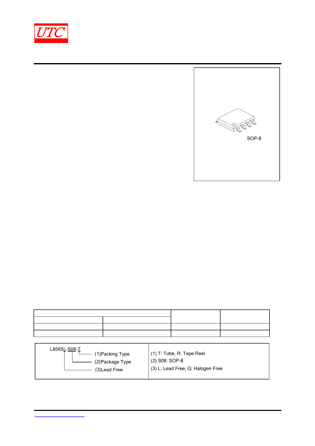
ORDERING INFORMATION
Ordering Number
Lead Free
Halogen Free
L8565L-S08-R
L8565G-S08-R
L8565L-S08-T
L8565G-S08-T
Package
SOP-8
SOP-8
Packing
Tape Reel
Tube
www.unisonic.com.tw
Copyright © 2013 Unisonic Technologies Co., Ltd
1 of 13
QW-R114-004.d
1 page 
L8565
Preliminary
LINEAR INTEGRATED CIRCUIT
ELECTRICAL CHARACTERISTICS(Cont.)
PARAMETER
SYMBOL
TEST CONDITIONS
MIN TYP MAX UNIT
SYSTEM PROTECTION SECTION
Open Loop Protection (OLP)
VSENSE Threshold
Peak Current Limitation (PCL)
ISENSE Threshold
Soft Over Current Control (SOC) ISENSE
Threshold
Output Under Voltage Detection (OUV)
VSENSE Threshold
Output Over-Voltage Protection (OVP)
VOLP
VPCL
VSOC
VOUV
VOVP
0.77 0.81 0.86 V
-1.15 -1.08 -1.00 V
-0.79 -0.73 -0.66 V
2.45 2.55 2.65
5.12 5.25 5.38
V
V
CURRENT LOOP SECTION
OTA2 Transconductance Gain
OTA2 Output Linear Range
ICOMP Voltage during OLP
GmOTA2
IOTA2
VICOMPF
At Temp=25°C
Guaranteed by design
VVSENSE=0.5V
0.9 1.1 1.3 mS
±50 µA
3.6 4.0
V
VOLTAGE LOOP SECTION
OTA1 Reference Voltage
OTA1 Transconductance Gain
OTA1 Max. Source Current Under
Normal Operation
OTA1 Max. Sink Current Under
Normal Operation
VOTA1
GmOTA1
IOTA1SO VVSENSE=4.25V, VVCOMP=4V
IOTA1SK VVSENSE=6V, VVCOMP=4V
4.90 5.00 5.10 V
31.5 42 52.5 µS
21 30 38 µA
21 30 38 µA
Soft Start End
OTA1 Source Current Under Soft Start
Enhanced Dynamic
Response
VSENSE High
VSENSE Low
VSENSE Input Bias Current At 5V
VSENSE Input Bias Current at 1V
VCOMP Voltage during OLP
VSOFT
IOTA1SS
VHi
VLo
IVSEN5V
IVSEN1V
VVCOMPF
VVSENSE=2V, VVCOMP=0V
VVSENSE=5V
VVSENSE=1V
VVSENSE= 0.5V, IVCOMP=0.5mA
3.80 4.00 4.20
8.0 10.8 13.4
5.12 5.25 5.38
4.63 4.75 4.87
0 1.5
01
0 0.2 0.4
V
µA
V
V
µA
µA
V
DRIVER SECTION
VCC=5V, IGATE=5mA
1.2 V
VCC=5V, IGATE=20mA
1.5 V
GATE Low Voltage
VGATEL IGATE=0A
0.8 V
IGATE=20mA
1.6 2.0 V
IGATE=-20mA
-0.2 0.2
V
VCC=20V, CL=4.7nF
11.5 V
GATE High Voltage
VGATEH VCC=11V, CL =4.7nF
10.5 V
VCC=VVCC(OFF)+0.2V, CL=4.7nF
7.5 V
GATE Rise Time
tR VGATE=2V...9V, CL=4.7nF
20 ns
GATE Fall Time
tF VGATE=9V...2V, CL=4.7nF
20 ns
GATE Current, Peak, Rising Edge
IGATE CL=4.7nF (Note 3)
-1.5 A
GATE Current, Peak, Falling Edge
IGATE CL=4.7nF (Note 3)
1.5 A
Notes: 1. Within the operating range the IC operates as described in the functional description.
2. The electrical characteristics involve the spread of values within the specified supply voltage and junction
temperature range TJ from -40°C to 125°C. Typical values represent the median values, which are related
to 25°C. If not otherwise stated, a supply voltage of VCC=15V is assumed for test condition.
3. Design characteristics (not meant for production testing)
UNISONIC TECHNOLOGIES CO., LTD
www.unisonic.com.tw
5 of 13
QW-R114-004.d
5 Page 
L8565
Preliminary
LINEAR INTEGRATED CIRCUIT
FUNCTIONAL DESCRIPTION(Cont.)
7. PWM Logic
The PWM logic block prioritizes the control input signals and generates the final logic signal to turn on the driver
stage. The speed of the logic gates in this block, together with the width of the reset pulse TOFF(MIN), are designed to
meet a maximum duty cycle DMAX of 95% at the GATE output under 133kHz of operation.
In case of high input currents which result in Peak Current Limitation, the GATE will be turned off immediately and
maintained in off state for the current PWM cycle. The signal TOFFMIN resets (highest priority, overriding other input
signals) both the current limit latch and the PWM on latch as illustrated in Fig. 13.
8. Voltage Loop
The voltage loop is the outer loop of the cascaded control scheme which controls the PFC output bus voltage VOUT.
This loop is closed by the feedback sensing voltage at VSENSE which is a resistive divider tapping from VOUT. The pin
VSENSE is the input of OTA1 which has an internal reference of 5V. Fig. 14 shows the important blocks of this voltage
loop.
8.1 Voltage Loop Compensation
The compensation of the voltage loop is installed at the VCOMP pin (see Fig. 14). This is the output of OTA1 and the
compensation must be connected at this pin to ground. The compensation is also responsible for the soft start
function which controls an increasing AC input current during start-up.
From L1
Full-wave
Retifier R7
D1 R3 VOUT
C2
R4
Current Loop
+
PWM Generation
VIN
Av(IIN)
Nonlinear
Gain
Gate Driver
GATE
-
OTA+1 5V
VSENSE
UTC L8565
VCOMP
R6
C4 C5
Fig. 14 Voltage Loop
UNISONIC TECHNOLOGIES CO., LTD
www.unisonic.com.tw
11 of 13
QW-R114-004.d
11 Page | ||
| Páginas | Total 13 Páginas | |
| PDF Descargar | [ Datasheet L8565.PDF ] | |
Hoja de datos destacado
| Número de pieza | Descripción | Fabricantes |
| L8560 | Low-Power SLIC with Ringing | Agere Systems |
| L8561 | POWER FACTOR CORRECTOR | Unisonic Technologies |
| L8562 | POWER FACTOR CORRECTOR | Unisonic Technologies |
| L8565 | HIGH PERFORMANCE POWER FACTOR CORRECTION CONTROLLER | Unisonic Technologies |
| Número de pieza | Descripción | Fabricantes |
| SLA6805M | High Voltage 3 phase Motor Driver IC. |
Sanken |
| SDC1742 | 12- and 14-Bit Hybrid Synchro / Resolver-to-Digital Converters. |
Analog Devices |
|
DataSheet.es es una pagina web que funciona como un repositorio de manuales o hoja de datos de muchos de los productos más populares, |
| DataSheet.es | 2020 | Privacy Policy | Contacto | Buscar |