|
|
PDF TVS8501V5 Data sheet ( Hoja de datos )
| Número de pieza | TVS8501V5 | |
| Descripción | TVS Diode ( Rectifier ) | |
| Fabricantes | ON Semiconductor | |
| Logotipo | ||
Hay una vista previa y un enlace de descarga de TVS8501V5 (archivo pdf) en la parte inferior de esta página. Total 6 Páginas | ||
|
No Preview Available !
TVS8501V5
Transient Voltage
Suppressors
Features
• Protection for the following IEC Standards:
IEC61000−4−2 Level 4: ±30 kV Contact Discharge
IEC61000−4−5 (Lightning) 70 A (8/20 ms)
• These Devices are Pb−Free, Halogen Free/BFR Free and are RoHS
Compliant
MAXIMUM RATINGS
Rating
Symbol
Value
Unit
IEC 61000−4−2 (ESD)
Contact
Air
±30 kV
±30
Operating Junction and Storage
Temperature Range
TJ, Tstg −65 to +150 °C
Maximum Peak Pulse Current
8/20 ms @ TA = 25°C
IPP 70 A
Stresses exceeding those listed in the Maximum Ratings table may damage the
device. If any of these limits are exceeded, device functionality should not be
assumed, damage may occur and reliability may be affected.
http://onsemi.com
1
Cathode
2
Anode
MARKING
DIAGRAM
UDFN2
CASE 517CZ
AM
A = Specific Device Code
M = Date Code
ORDERING INFORMATION
Device
Package
Shipping†
TVS8501V5MUT5G UDFN2 8000 / Tape &
(Pb−Free)
Reel
†For information on tape and reel specifications,
including part orientation and tape sizes, please
refer to our Tape and Reel Packaging Specifications
Brochure, BRD8011/D.
© Semiconductor Components Industries, LLC, 2014
November, 2014 − Rev. 1
1
Publication Order Number:
TVS8501V5/D
1 page 
TVS8501V5
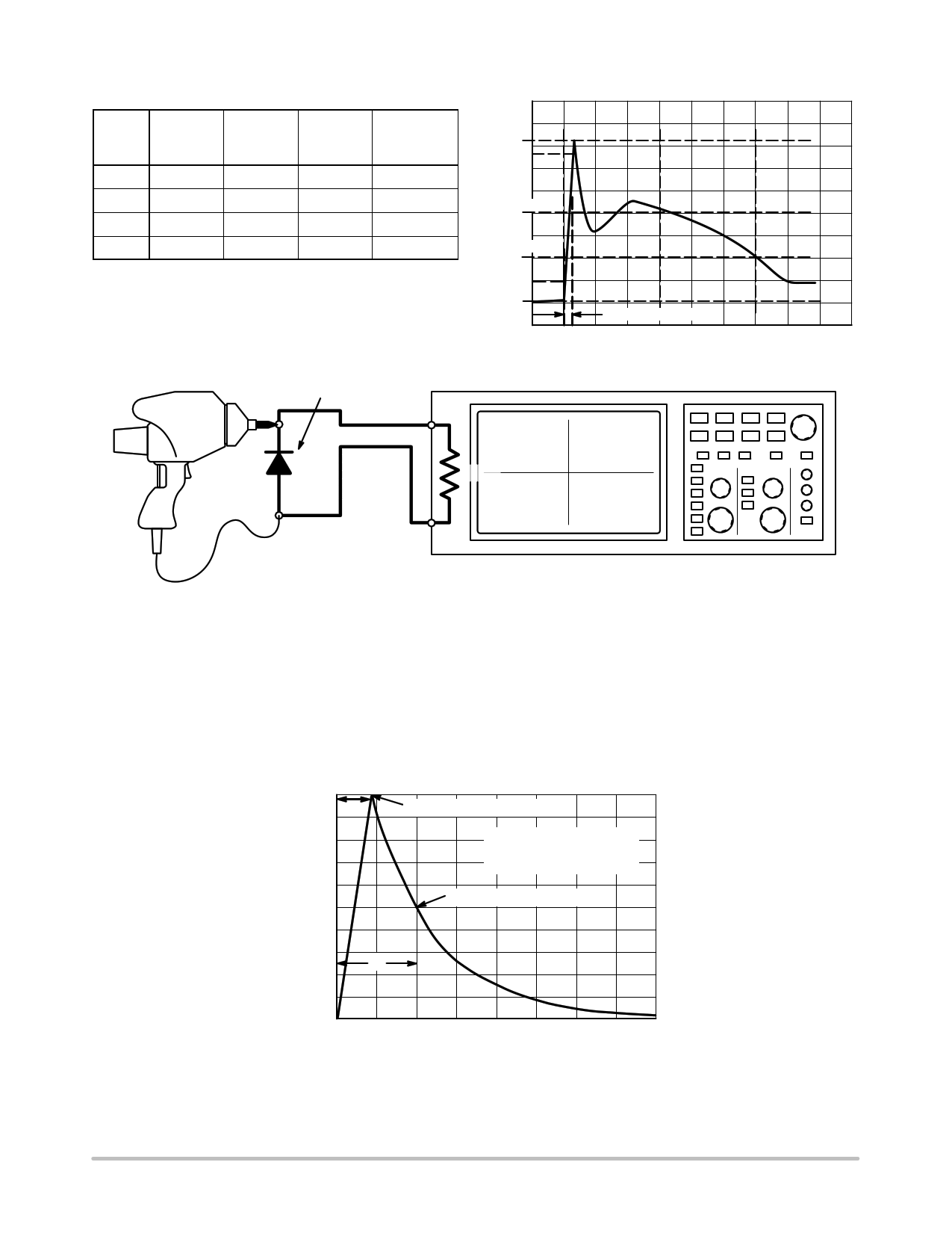
IEC 61000−4−2 Spec.
Level
First Peak
Test Volt- Current Current at
age (kV)
(A) 30 ns (A)
1 2 7.5 4
2 4 15 8
3 6 22.5 12
48
30 16
Current at
60 ns (A)
2
4
6
8
IEC61000−4−2 Waveform
Ipeak
100%
90%
I @ 30 ns
I @ 60 ns
10%
Figure 6. IEC61000−4−2 Spec
tP = 0.7 ns to 1 ns
ESD Gun
TVS
Oscilloscope
50 W
Cable
50 W
Figure 7. Diagram of ESD Test Setup
ESD Voltage Clamping
For sensitive circuit elements it is important to limit the
voltage that an IC will be exposed to during an ESD event
to as low a voltage as possible. The ESD clamping voltage
is the voltage drop across the ESD protection diode during
an ESD event per the IEC61000−4−2 waveform. Since the
IEC61000−4−2 was written as a pass/fail spec for larger
systems such as cell phones or laptop computers it is not
clearly defined in the spec how to specify a clamping voltage
at the device level. ON Semiconductor has developed a way
to examine the entire voltage waveform across the ESD
protection diode over the time domain of an ESD pulse in the
form of an oscilloscope screenshot, which can be found on
the datasheets for all ESD protection diodes. For more
information on how ON Semiconductor creates these
screenshots and how to interpret them please refer to
AND8307/D.
100
tr
90
80
70
60
50
40
30
20
10
0
0
PEAK VALUE IRSM @ 8 ms
PULSE WIDTH (tP) IS DEFINED
AS THAT POINT WHERE THE
PEAK CURRENT DECAY = 8 ms
HALF VALUE IRSM/2 @ 20 ms
tP
20 40
60
t, TIME (ms)
Figure 8. 8 X 20 ms Pulse Waveform
80
http://onsemi.com
5
5 Page | ||
| Páginas | Total 6 Páginas | |
| PDF Descargar | [ Datasheet TVS8501V5.PDF ] | |
Hoja de datos destacado
| Número de pieza | Descripción | Fabricantes |
| TVS8501V12 | TVS Diode ( Rectifier ) | ON Semiconductor |
| TVS8501V5 | TVS Diode ( Rectifier ) | ON Semiconductor |
| TVS8501V6 | TVS Diode ( Rectifier ) | ON Semiconductor |
| Número de pieza | Descripción | Fabricantes |
| SLA6805M | High Voltage 3 phase Motor Driver IC. |
Sanken |
| SDC1742 | 12- and 14-Bit Hybrid Synchro / Resolver-to-Digital Converters. |
Analog Devices |
|
DataSheet.es es una pagina web que funciona como un repositorio de manuales o hoja de datos de muchos de los productos más populares, |
| DataSheet.es | 2020 | Privacy Policy | Contacto | Buscar |
