|
|
|
PDF ISL55033 Data sheet ( Hoja de datos )
| Número de pieza | ISL55033 | |
| Descripción | Rail-to-Rail Output Gain Block | |
| Fabricantes | Intersil | |
| Logotipo | ||
Hay una vista previa y un enlace de descarga de ISL55033 (archivo pdf) en la parte inferior de esta página. Total 13 Páginas | ||
|
No Preview Available !
DATASHEET
400MHz Slew Rate Enhanced, Rail-to-Rail Output Gain
Block
ISL55033
The ISL55033 is a triple rail-to-rail output gain block with a
-3dB bandwidth of 400MHz and slew rate of 2350V/µs into a
150 load. The ISL55033 has a fixed gain of +2. The inputs
are capable of sensing ground. The outputs are capable of
swinging to 0.45V to either rail through a 150Ω resistor
connected to V+/2.
The ISL55033 is designed for general purpose video
applications. The part includes a fast-acting global
disable/power-down function.
The ISL55033 is available in a 12 Ld TQFN package. Operation
is specified over the -40°C to +85°C temperature range.
Features
• 400MHz -3dB bandwidth
• 2350V/µs typ slew rate, RL = 150Ωto V+/2
• Single-supply operation from +3V to +5.5V
• Rail-to-rail output
• Input ground sensing
• Fast 25ns disable time
• Pb-free (RoHS compliant)
Applications
• Video amplifiers
• Set-top boxes
• Video distribution
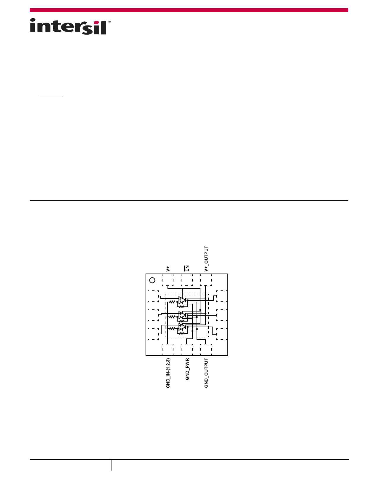
Pin Configuration
ISL55033
(12 LD TQFN)
TOP VIEW
12 11 10
IN+_1 1
9 OUTPUT_1
IN+_2 2
IN+_3 3
4
8 OUTPUT_2
EP 7 OUTPUT_3
56
EACH CHANNEL
AV = +2
June 29, 2015
FN6346.1
1
CAUTION: These devices are sensitive to electrostatic discharge; follow proper IC Handling Procedures.
1-888-INTERSIL or 1-888-468-3774 | Copyright Intersil Americas LLC 2008, 2015. All Rights Reserved
Intersil (and design) is a trademark owned by Intersil Corporation or one of its subsidiaries.
All other trademarks mentioned are the property of their respective owners.
1 page 
ISL55033
Typical Performance Curves
3
RL = 1k
2
RL = 499
1
0
-1
-2
-3 V+ = V+_OUT = 5V
AV = +2
-4 CL = 2pF
-5
VOUT = 100mVP-P
VIN(DC) = 0.1V
RL = 150
RL = 100
-6
100k
1M
10M
100M
1G
FREQUENCY (Hz)
FIGURE 1. GAIN vs FREQUENCY FOR VARIOUS RLOAD
8
CL = 9.2pF
6
CL = 7.8pF
4
CL = 5.7pF
2 CL = 4.3pF
0
-2
V+ = V+_OUT = 5V
-4 AV = +2
RL = 150Ω
-6 VOUT = 100mVP-P
VIN(DC) = 0.1V
-8
100k
1M
CL = 3.2pF
CL = 2.0pF
10M
100M
1G
FREQUENCY (Hz)
FIGURE 2. GAIN vs FREQUENCY FOR VARIOUS CLOAD
1
0
-1
-2 VOUT = 0.1VP-P
-3 VOUT = 0.5VP-P
-4
-5
-6
V+ = V+_OUT = 5V
AV = +2
-7 RL = 150Ω
-8
CL = 2pF
VIN(DC) = 0.1V
-9
100k
1M
VOUT = 1.0VP-P
VOUT = 1.5VP-P
10M
100M
FREQUENCY (Hz)
1G
FIGURE 3. GAIN vs FREQUENCY FOR VARIOUS VOUT
7
6
ALL CHANNELS
5
4
3
V+ = V+_OUT = 5V
2
AV = +2
RL = 150Ω
1
CL = 2pF
VOUT = 100mVP-P
VIN(DC) = 0.1V
0
10k 100k
1M
10M
FREQUENCY (Hz)
100M
1G
FIGURE 5. GAIN vs FREQUENCY - ALL CHANNELS
4
2
0
VIN(DC) = 2.3V
-2
VIN(DC) = 2.2V
VIN(DC) = 2.0V
-4
VIN(DC) = 1.0V
VIN(DC) = 0.1V
-6 V+ = V+_OUT = 5V
AV = +2
-8
RL = 150Ω
CL = 2pF
VOUT = 100mVP-P
-10
100k
1M
10M
FREQUENCY (Hz)
100M
1G
FIGURE 4. GAIN vs FREQUENCY FOR VARIOUS DC INPUT VOLTAGES
0.2
0.1
0
-0.1
-0.2
-0.3
-0.4 V+ = V+_OUT = 5V
-0.5 AV = +2
-0.6
RL = 150Ω
CL = 2pF
-0.7
VOUT = 100mVP-P
VIN(DC) = 0.1V
-0.8
10k
100k
1M
FREQUENCY (Hz)
10M
FIGURE 6. 0.1 dB GAIN FLATNESS
100M
Submit Document Feedback
5
FN6346.1
June 29, 2015
5 Page 
ISL55033
Application Information
General
The ISL55033 single supply, fixed gain, triple amplifier is
intended for use in a variety of video and other high speed
applications. The device features a ground-sensing PNP input
stage and a bipolar rail-to-rail output stage. The three amplifiers
have an internally fixed gain of 2 and share a single enable pin as
shown in Figure 32.
Ground Connections
For the best isolation performance and crosstalk rejection, all
GND pins must connect directly to the GND plane. In addition, the
electrically conductive thermal pad (EP) must also connect
directly to ground.
Power Considerations
Separate V+ power supply and GND pins for the input and output
stages are provided to maximize PSRR. Providing separate
power pins provides a way to prevent high speed transient
currents in the output stage from bleeding into the sensitive
amplifier input and gain stages. To maximize crosstalk isolation,
each power supply pin should have its own decoupling capacitors
connected as close to the pin as possible as shown in Figure 32
(0.1µF in parallel with 1nF recommended).
The ESD protection circuits use internal diodes from all pins to the
V+ and ground pins. In addition, a dV/dt-triggered clamp is
connected between the V+ and V- pins, as shown in Equivalent
Circuit 1 on page 2. The dV/dt triggered clamp imposes a
maximum supply turn-on slew rate of 1V/µs. Damaging currents
can flow for power supply slew rates in excess of 1V/µs, such as
during hot plugging. Under these conditions, additional methods
should be employed to ensure the maximum supply slew rate is
not exceeded.
Single Supply Input/Output Considerations
For best performance, the input signal voltage range should be
maintained between 0.1V to 2.1V. These input limits correspond
to an output voltage range of 0.2V to 4.2V and define the limits
of linear operation. Figure 4 shows the frequency response
versus the input DC voltage level. Figures 16 and 17 show the
differential gain-phase performance over the input range of 0V to
2.4V operating into a 150Ω load. The 0.1V to 2.1V input levels
corresponds to a 0.2V to 4.2V output levels, which define the
minimum and maximum range of output linear operation.
Composite video with sync requires care to ensure that the
negative sync tip voltage (typically -300mV) is properly
level-shifted up into the ISL55033 input linear operating region
of +0.1V to 2.1V. The high input impedance enables AC coupling
using low values of coupling capacitance with relatively high
input voltage divider resistances.
EN and Power-down States
The EN pin is active low. An internal pull-down resistor ensures
the device will be active with no connection to the EN pin. The
power-down state is established within approximately 25ns, if a
logic high (>2V) is placed on the EN pin. In the power-down state,
supply current is reduced significantly by shutting the three
amplifiers off. The output presents a relatively high impedance
(~2kΩ) to the output pin. Multiplexing several outputs together is
possible using the enable/disable function as long as the
application can tolerate the limited power-down output
impedance.
Limiting the Output Current
No output short-circuit current limit exists on these parts. All
applications need to limit the output current to less than 40mA.
Adequate thermal heat sinking of the parts is also required.
PC Board Layout
The AC performance of this circuit depends greatly on the care
taken in designing the PC board. The following are
recommendations to achieve optimum high frequency
performance from your PC board.
• The use of low inductance components, such as chip resistors
and chip capacitors, is strongly recommended.
• Minimize signal trace lengths. Trace inductance and
capacitance can easily limit circuit performance. Avoid sharp
corners. Use rounded corners when possible. Vias in the signal
lines add inductance at high frequency and should be avoided.
PCB traces greater than 1" begin to exhibit transmission line
characteristics with signal rise/fall times of 1ns or less. High
frequency performance may be degraded for traces greater
than one inch, unless controlled impedance (50Ωor75Ωstrip
lines or microstrips are used.
• Match channel-to-channel analog I/O trace lengths and layout
symmetry. This will minimize propagation delay mismatches.
• Maximize use of AC decoupled PCB layers. All signal I/O lines
should be routed over continuous ground planes (i.e. no split
planes or PCB gaps under these lines). Avoid vias in the signal I/O
lines.
• Use proper value and location of termination resistors. Input
termination resistors should be as close to the input terminal as
possible and output termination resistors as close to the receiving
device as possible.
• When testing, use good quality connectors and cables, matching
cable types and keeping cable lengths to a minimum.
• A minimum of two, high frequency, power supply decoupling
capacitors (1000pF, 0.1µF), on each V+ pin, are recommended as
close to the devices as possible. Avoid vias between the capacitor
and the device because vias add unwanted inductance. Larger
capacitors (e.g., electrolytics) can be farther away. When vias are
required in a layout, they should be routed as far away from the
device as possible.
Submit Document Feedback 11
FN6346.1
June 29, 2015
11 Page | ||
| Páginas | Total 13 Páginas | |
| PDF Descargar | [ Datasheet ISL55033.PDF ] | |
Hoja de datos destacado
| Número de pieza | Descripción | Fabricantes |
| ISL55033 | Rail-to-Rail Output Gain Block | Intersil |
| ISL55036 | 400MHz Slew Rate Enhanced Rail-to-Rail Output Gain Block | Intersil |
| Número de pieza | Descripción | Fabricantes |
| SLA6805M | High Voltage 3 phase Motor Driver IC. |
Sanken |
| SDC1742 | 12- and 14-Bit Hybrid Synchro / Resolver-to-Digital Converters. |
Analog Devices |
|
DataSheet.es es una pagina web que funciona como un repositorio de manuales o hoja de datos de muchos de los productos más populares, |
| DataSheet.es | 2020 | Privacy Policy | Contacto | Buscar |