|
|
PDF ISL55210 Data sheet ( Hoja de datos )
| Número de pieza | ISL55210 | |
| Descripción | Ultra-High Dynamic Range Differential Amplifier | |
| Fabricantes | Intersil | |
| Logotipo |  |
|
Hay una vista previa y un enlace de descarga de ISL55210 (archivo pdf) en la parte inferior de esta página. Total 18 Páginas | ||
|
No Preview Available !
Wideband, Low-Power, Ultra-High Dynamic Range
Differential Amplifier
ISL55210
The ISL55210 is a very wide band, Fully Differential Amplifier
(FDA) intended for high dynamic range ADC input interface
applications. This voltage feedback FDA design includes an
independent output common mode voltage control.
Intended for very high dynamic range ADC interface
applications, at the lowest quiescent power (115mW), the
ISL55210 offers a 4.0GHz Gain Bandwidth Product with a very
low input noise of 0.85nV/√(Hz). In a balanced differential I/O
configuration, with 2VP-P output into a 200Ω load configured
for a gain of 15dB, the IM3 terms are <-100dBc through
110MHz. With a minimum operating gain of 2V/V (6dB), the
ISL55210 supports a wide range of higher gains with minimal
BW or SFDR degradation. Its ultra high differential slew rate of
5,600V/µs ensures clean large signal SFDR performance or a
fast settling step response.
The ISL55210 requires only a single 3.3V (max 4.2V) power
supply with 35mA typical quiescent current. This industry
leading low current solution can be further reduced when
needed using the optional power shutdown to <0.4mA supply
current. External feedback and gain setting resistors give
maximum flexibility and accuracy. A companion device, the
ISL55211, includes on-chip feedback and 3 possible gain
setting connections where an internally fixed gain solution is
preferred. The ISL55210 is available in a leadless, 16 Ld TQFN
package and is specified for operation over the -40ºC to +85ºC
ambient temperature range.
Features
• Gain Bandwidth Product . . . . . . . . . . . . . . . . . . . . . . . . 4.0GHz
• Input Voltage Noise . . . . . . . . . . . . . . . . . . . . . . . 0.85nV/√(Hz)
• Differential Slew Rate . . . . . . . . . . . . . . . . . . . . . . . 5,600V/µs
• 2VP-P, 2-tone IM3 (200Ω) 100MHz . . . . . . . . . . . . . . -109dBc
• Supply Voltage Range . . . . . . . . . . . . . . . . . . . . . . 3.0V to 4.2V
• Quiescent Power (3.3V Supply) . . . . . . . . . . . . . . . . . .115mW
Applications
• Low Power, High Dynamic Range ADC Interface
• Differential Mixer Output Amplifier
• SAW Filter Pre/Post Driver
• Differential Comms-DAC Output Driver
Related Products and
Literature
• ISL55211 - Fixed Gain Version of the ISL55210
• ISLA112P50 - 12-bit, 500MSPS ADC (<500mW)
• ISLA214P50 - 14-bit, 500MSPS ADC (<850mW)
• AN1649 - Designer’s Guide to the ISL55210 and ISL55211
Evaluation Boards
• AN1725 - Ultra Low Power Broadband 8 to 14-Bit Data
Acquisition Platform
• AN1837 - Ultra High Performance Broadband 12 to 16-Bit
Data Acquisition Platform
• AN1831 - Designer's Guide to the ISL55210-ABEVAL1Z
Active Balun Evaluation Board
105MHz SINGLE TONE
180mVpp for -1dBFS
100
Vi 1:2
0.1µF
50
Vcm
+3.3V
35mA
495 (115mW)
10k
500kHz 180MHz SPAN
ISLA112P50
+
40.2
12 Bit
V+ <500mW
0.1µF
33nH
20pF
PD
ISL55210
Vb 210
Vdiff
ADT4-1WT
100
-
495
0.1µF
210
33nH
20pF
V-
40.2
500MSPS
Vdiff
20log ( Vi ) = 17.3dB gain
CLK
FIGURE 1. TYPICAL APPLICATION CIRCUIT
SNRFS = 64.9dBFS
HD2 = -83dBc
HD3 = -84dBc
ENOBFS = 10.5 Bits
June 6, 2013
FN7811.2
1
CAUTION: These devices are sensitive to electrostatic discharge; follow proper IC Handling Procedures.
1-888-INTERSIL or 1-888-468-3774 |Copyright Intersil Americas LLC 2011-2013. All Rights Reserved
Intersil (and design) is a trademark owned by Intersil Corporation or one of its subsidiaries.
All other trademarks mentioned are the property of their respective owners.
1 page 
ISL55210
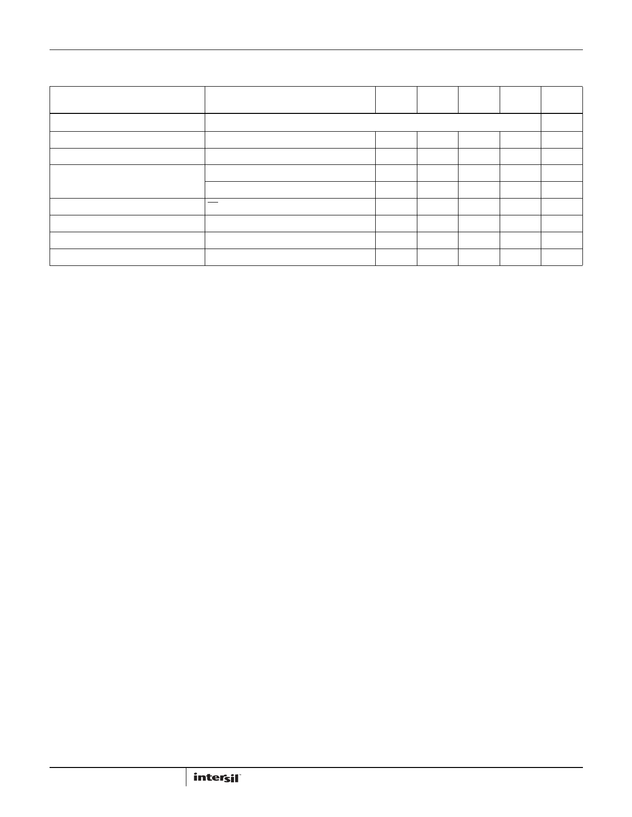
Electrical Specifications VS+ = +3.3V Test Conditions: G = 12dB, VCM = open, VO = 2VP-P, RF = 200Ω, RL = 200Ω differential, TA = +25°C,
differential input, differential output, input and output referenced to internal default VCM (1.2V nominal) unless otherwise specified. (Continued)
PARAMETER
CONDITIONS
MIN
MAX
TESTED
(Note 6) TYP (Note 6) UNIT (Note 7)
POWER-DOWN
Referenced to GND
Enable Voltage Threshold
Assured on above 1.55V
1.3 1.55
V
*
Disable Voltage Threshold
Assured off below 0.54V
0.54
0.7
V*
Power-down Quiescent Current
Input Bias Current
TA = +25°C
TA = -40°C to +85°C
PD = 0V, current positive into pin
0.2 0.3 0.4 mA
0.15 0.3 0.45 mA
-2 µA
*
Input Impedance
2 || 5
MΩ || pF
Turn-on Time Delay
Measured to output on
200 ns
Turn-off Time Delay
Measured to output off
400 ns
NOTES:
6. Compliance to datasheet limits is assured by one or more methods: production test, characterization, and/or design.
7. Parameters denoted by an “*” are ATE tested.
5 FN7811.2
June 6, 2013
5 Page 
ISL55210
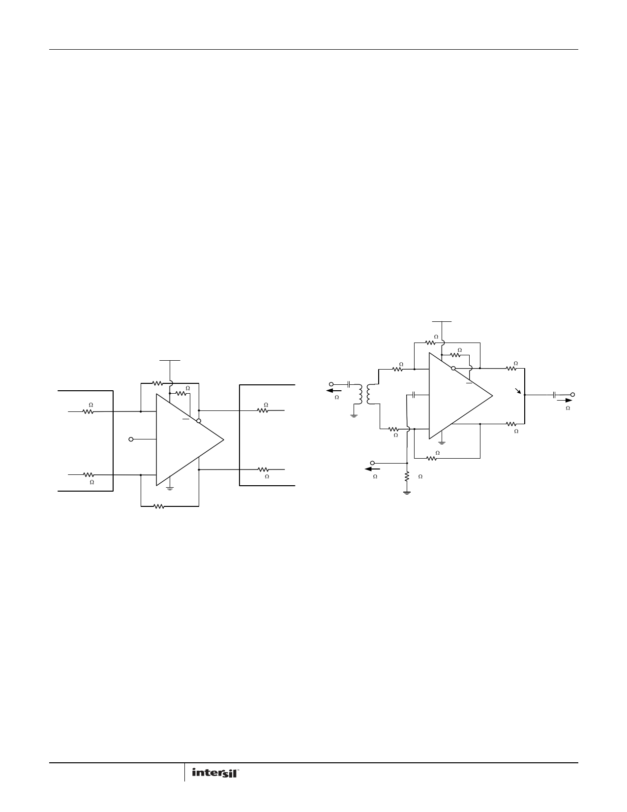
Most of the characterization curves start with Figure 28 then get
different gains by changing the feedback resistor, RF, use
different input transformers where then the RG is also adjusted
to hold an input match, or vary the loading. For load tests below
the 200Ω shown in Figure 28, a simple added shunt resistor is
placed across the output pins. For loads >200Ω, the series and
shunt load R's are adjusted to show that total load (including the
50Ω measurement load reflected through the 1:1 output
measurement port transformer) and provide an apparent 50Ω
differential source to that transformer. This output side
transformer is for measurement purposes only and is not
necessary for final applications circuits. There are output
interface designs that do benefit from a transformer as part of
the signal path, but the one shown at the right of Figure 28 is
used only for characterization to get a doubly terminated 50Ω
measurement path going differential to single ended.
Where just the amplifier is tested, a 4 port network analyzer is
used and the very simple test circuit of Figure 29 is
implemented. This is used to extract the differential S21 curves
and differential output impedance vs gain. Changing the gain is a
simple matter of adjusting the two RF resistors of Figure 29. This
circuit depends on the two AC coupled source 50Ω of the 4 port
network analyzer and presents an AC coupled differential 100Ω
load to the amplifier as the input impedance of the remaining
two ports of the network analyzer.
+3.3V
RF
10k
50
1/2 OF A 4-port
S-PARAMETER
VCM
+
PD
ISL55210
50
1/2 OF A 4-PORT
S-PARAMETER
-
50
50
impedance that increases with signal gain setting. The ISL55210
holds a more constant response vs gain due to internal design
elements unique to this device.
Common mode output measurements are made using the circuit
Figure 30. Here, the outputs are summed together through two
100Ω resistors (still a 200Ω differential load) to a center point
where the average, or common mode, output voltage may be
sensed. This is coupled through a 1µF DC blocking capacitor and
measured using 50Ω test equipment. The common mode source
impedance for this circuit is the parallel combination of the
2Ω - 100Ω elements, or 50Ω. Figure 18 uses this circuit to
measure the small and large signal response from the VCM
control pin to the output common mode. This pin includes an
internal 50pF capacitor on the default bias network (to filter
supply noise when there is no connection to this pin) which
bandlimits the response to approximately 30MHz. This is far
lower than the actual bandwidth of the common mode loop.
Figure 19 uses this output CM measurement circuit with a large
signal (2VP-P) differential output voltage (generated through the
Vi path of Figure 30) to measure the differential to common
mode conversion.
+3.3V
Vi 1:1.4
50 1µF
ADT2-1T
50
50
VCM INPUT
200
10k
+
PD
VCM ISL55210
-
200
100
OUTPUT
VCM
100
1µF
50
50 50
RF
FIGURE 29. TEST CIRCUIT #2 4-PORT S-PARAMETER
MEASUREMENTS
Using this measurement allows the full small single bandwidth of
the ISL55210 to be exposed. Many of the other measurements are
using I/O transformers that are limiting the apparent bandwidth to
reduced level. Figure 16 shows a series of normalized differential
S21 curves for gains of 12dB to 30dB in 6dB steps. These are
simply stepping two feedback resistor values (RF) up from 200Ω to
1600Ω in 2X steps. The lowest gain of 12dB (4V/V) is showing a
2.2GHz small signal bandwidth. This response gets some
bandwidth extension due to phase margin <60degree effects, but
by the gain of 24dB (16V/V), the bandwidth is following a Gain
Bandwidth type characteristic showing 300MHz bandwidth or
>4GHz Gain Bandwidth Product (GBP).
The closed loop differential output impedance of Figure 17 is
simulated using Figure 29 in ADS. This shows a relatively low
output impedance (<1Ω through 100MHz) constant with signal
gain setting. Typical FDA outputs show a closed loop output
FIGURE 30. TEST CIRCUIT #3 COMMON MODE AC OUTPUT
MEASUREMENTS
Single Supply, Input Transformer Coupled,
Design Considerations
The characterization circuit of Figure 28 shows one possible
input stage interface that offers several advantages. The
ISL55210 can also support a DC coupled differential to
differential or single ended input to differential requirement if
needed. Where AC coupling is adequate, the circuit of Figure 28
simplifies the input common mode voltage control. If the source
coming into this stage is single ended, the input transformer
provides a zero power conversion to differential. The two gain
resistors (RG in Figure 28) provide both the input termination
impedance and the gain element for the amplifier. For minimum
noise, only RG should be used and set to achieve the desired
input impedance. Since the ISL55210 is a VFA device, these
resistor values can be scaled up and down a bit more freely than
a current feedback based FDA.
11 FN7811.2
June 6, 2013
11 Page | ||
| Páginas | Total 18 Páginas | |
| PDF Descargar | [ Datasheet ISL55210.PDF ] | |
Hoja de datos destacado
| Número de pieza | Descripción | Fabricantes |
| ISL55210 | Ultra-High Dynamic Range Differential Amplifier | Intersil |
| ISL55211 | Differential Amplifier | Intersil |
| Número de pieza | Descripción | Fabricantes |
| SLA6805M | High Voltage 3 phase Motor Driver IC. |
Sanken |
| SDC1742 | 12- and 14-Bit Hybrid Synchro / Resolver-to-Digital Converters. |
Analog Devices |
|
DataSheet.es es una pagina web que funciona como un repositorio de manuales o hoja de datos de muchos de los productos más populares, |
| DataSheet.es | 2020 | Privacy Policy | Contacto | Buscar |
