|
|
|
PDF NDT02N60Z Data sheet ( Hoja de datos )
| Número de pieza | NDT02N60Z | |
| Descripción | N-Channel Power MOSFET / Transistor | |
| Fabricantes | ON Semiconductor | |
| Logotipo | ||
Hay una vista previa y un enlace de descarga de NDT02N60Z (archivo pdf) en la parte inferior de esta página. Total 6 Páginas | ||
|
No Preview Available !
NDT02N60Z
N-Channel Power MOSFET
600 V, 8.0 W
Features
• 100% Avalanche Tested
• Extremely High dv/dt Capability
• Gate Charge Minimized
• Zener−protected
• These Devices are Pb-Free, Halogen Free/BFR Free and are RoHS
Compliant
ABSOLUTE MAXIMUM RATINGS (TJ = 25°C unless otherwise noted)
Parameter
Symbol Value Unit
Drain−to−Source Voltage
Gate−to−Source Voltage
Continuous Drain Current RqJA
Steady State, TC = 25°C
VDSS 600 V
VGS ±30 V
ID 0.3 A
Continuous Drain Current RqJA
Steady State, TC = 100°C
ID 0.21 A
Power Dissipation – RqJA
Steady State, TC = 25°C
Pulsed Drain Current
Continuous Source Current (Body Diode)
Single Pulse Drain−to−Source Avalanche
Energy (ID = 1.4 A)
PD
IDM
IS
EAS
2.0 W
5A
2.2 A
38 mJ
Peak Diode Recovery (Note 1)
dV/dt
4.5 V/ns
Maximum Temperature for Soldering Leads
TL
Operating Junction and Storage Temperature TJ, TSTG
260
−55 to
+150
°C
°C
Stresses exceeding those listed in the Maximum Ratings table may damage the
device. If any of these limits are exceeded, device functionality should not be
assumed, damage may occur and reliability may be affected.
1. IS < 2.2 A, di/dt ≤ 200 A/ms, VDD ≤ BVDSS, TJ = +150°C
THERMAL RESISTANCE
Parameter
Symbol Value Unit
Junction−to−Ambient Steady State
NDT02N60Z (Note 2)
NDT02N60Z (Note 3)
RqJA
°C/W
61
148
2. Surface mounted on FR4 board using 1″ sq. pad size
(Cu area = 1.127″ sq. [2 oz] including traces)
3. Surface−mounted on FR4 board using minimum recommended pad size
(Cu area = 0.026” sq. [2 oz]).
http://onsemi.com
V(BR)DSS
600 V
RDS(ON) MAX
8.0 W @ 10 V
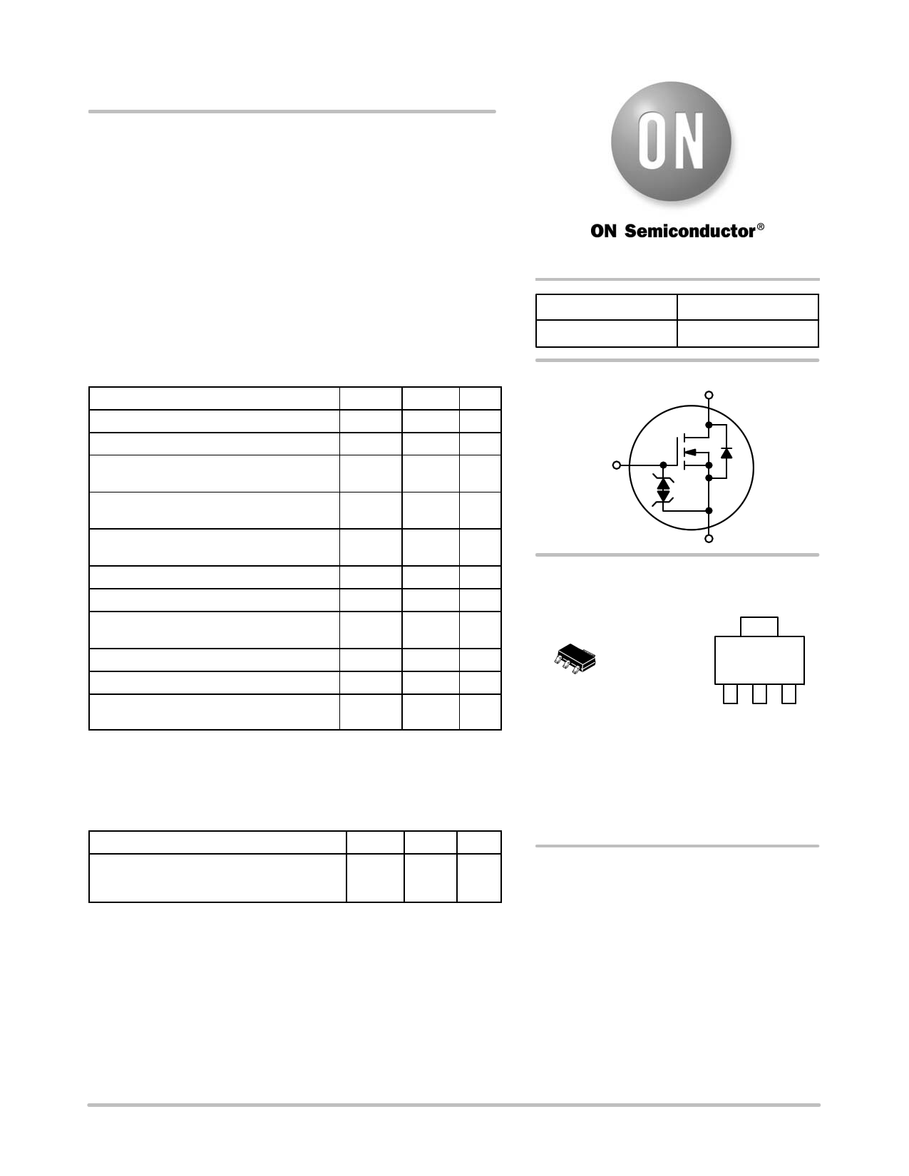
N−Channel
D (2, 4)
G (1)
S (3)
4
1 23
SOT−223
CASE 318E
STYLE 3
MARKING
DIAGRAM
Drain
4
AYW
2N60ZG
G
12 3
Gate Drain Source
A = Assembly Location
Y = Year
W = Work Week
2N60Z = Specific Device Code
G = Pb−Free Package
(Note: Microdot may be in either location)
ORDERING INFORMATION
See detailed ordering and shipping information in the package
dimensions section on page 5 of this data sheet.
© Semiconductor Components Industries, LLC, 2014
May, 2014 − Rev. 0
1
Publication Order Number:
NDT02N60Z/D
1 page 
NDT02N60Z
100
Duty Cycle = 0.5
0.2
10 0.1
0.05
0.02
1
0.01
0.1
Single Pulse
0.01
1E−06
1E−05
TYPICAL CHARACTERISTICS
100
VGS ≤ 30 V
Single Pulse
10 TC = 25°C
1
0.1
10 ms
100 ms
1 ms
10 ms
0.01
RDS(on) Limit
Thermal Limit
Package Limit
dc
0.001
0.1 1
10 100 1000
VDS, DRAIN−TO−SOURCE VOLTAGE (V)
Figure 13. Maximum Rated Forward Biased
Safe Operating Area
RqJA = Steady State = 61°C/W
1E−04
1E−03
1E−02
1E−01
1E+00
t, TIME (s)
Figure 14. Thermal Impedance (Junction−to−Ambient)
1E+01
1E+02 1E+03
ORDERING INFORMATION
Device
Package
Shipping†
NDT02N60ZT1G
NDT02N60ZT3G
SOT−223
(Pb−Free, Halogen Free)
1000 / Tape & Reel
4000 / Tape & Reel
†For information on tape and reel specifications, including part orientation and tape sizes, please refer to our Tape and Reel Packaging
Specifications Brochure, BRD8011/D.
http://onsemi.com
5
5 Page | ||
| Páginas | Total 6 Páginas | |
| PDF Descargar | [ Datasheet NDT02N60Z.PDF ] | |
Hoja de datos destacado
| Número de pieza | Descripción | Fabricantes |
| NDT02N60Z | N-Channel Power MOSFET / Transistor | ON Semiconductor |
| Número de pieza | Descripción | Fabricantes |
| SLA6805M | High Voltage 3 phase Motor Driver IC. |
Sanken |
| SDC1742 | 12- and 14-Bit Hybrid Synchro / Resolver-to-Digital Converters. |
Analog Devices |
|
DataSheet.es es una pagina web que funciona como un repositorio de manuales o hoja de datos de muchos de los productos más populares, |
| DataSheet.es | 2020 | Privacy Policy | Contacto | Buscar |