|
|
PDF 6ED003L06-F2 Data sheet ( Hoja de datos )
| Número de pieza | 6ED003L06-F2 | |
| Descripción | High voltage gate driver IC | |
| Fabricantes | Infineon | |
| Logotipo |  |
|
Hay una vista previa y un enlace de descarga de 6ED003L06-F2 (archivo pdf) en la parte inferior de esta página. Total 20 Páginas | ||
|
No Preview Available !
EiceDRIVER™
High voltage gate driver IC
6ED family - 2nd generation
3 phase 600 V gate drive IC
6ED003L06-F2
6ED003L02-F2
EiceDRIVER™
datasheet
<Revision 2.8>, 05.08.2016
Industrial Power Control
1 page 
EiceDRIVER™
6ED003L06-F2, 6ED003L02-F2
EiceDRIVER™
3 phase 600 V gate drive IC
1 Overview
Main features
Thin-film-SOI-technology
Maximum blocking voltage +600V
Separate control circuits for all six drivers
CMOS and LSTTL compatible input (negative logic)
Signal interlocking of every phase to prevent cross-conduction
Detection of over current and under voltage supply
externally programmable delay for fault clear after over current
detection
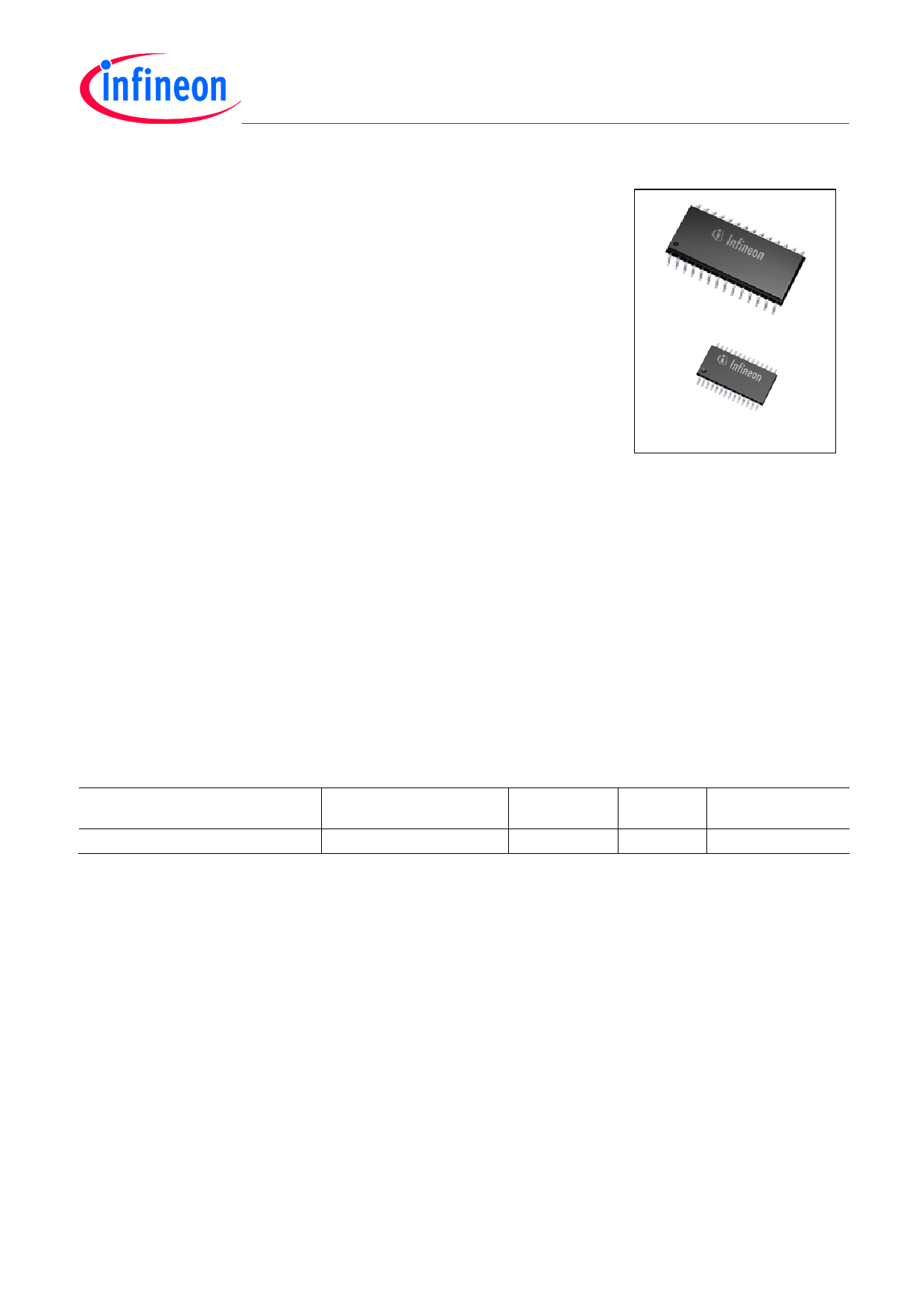
PG-DSO28
PG-TSSOP28
Product highlights
Insensitivity of the bridge output to negative transient voltages up to -50V given by SOI-technology
'shut down' of all switches during error conditions
Typical applications
Home appliances
Fans, pumps
General purpose drives
Product family
Table 1
Members of 6ED family – 2nd generation
Sales Name
high side control input
HIN1,2,3 and LIN1,2,3
6ED003L06-F2 / 6ED003L02-F2 negative logic
typ. UVLO- Bootstrap Package
Thresholds diode
11.7 V / 9.8 V No
DSO28 / TSSOP28
Description
The devices are full bridge drivers to control power devices like MOS-transistors or IGBTs in 3-phase systems
with a maximum blocking voltage of +600 V. Based on the used SOI-technology there is an excellent
ruggedness on transient voltages. No parasitic thyristor structures are present in the device. Hence, no parasitic
latch-up may occur at all temperatures and voltage conditions.
The six independent drivers are controlled at the low-side using CMOS resp. LSTTL compatible signals, down
to 3.3 V logic. The device includes an under-voltage detection unit with hysteresis characteristic and an over-
current detection. The over-current level is adjusted by choosing the resistor value and the threshold level at pin
ITRIP. Both error conditions (under-voltage and over-current) lead to a definite shut down of all six switches. An
error signal is provided at the FAULT open drain output pin. The blocking time after over-current can be
adjusted with an RC-network at pin RCIN. The input RCIN owns an internal current source of 2.8 µA. Therefore,
the resistor RRCIN is optional. The typical output current can be given with 165 mA for pull-up and 375 mA for pull
down. Because of system safety reasons a 310 ns interlocking time has been realised. The function of input EN
can optionally be extended with an over-temperature detection, using an external NTC-resistor (see Fig.1).
datasheet
5 <Revision 2.8>, 05.08.2016
5 Page 
EiceDRIVER™
6ED003L06-F2, 6ED003L02-F2
4.2 Required operation conditions
All voltages are absolute voltages referenced to VSS -potential unless otherwise specified. All parameters are
valid for Ta=25 °C.
Table 4
Required Operation Conditions
Parameter
High side offset voltage (Note 1)
Low side supply voltage (VCC vs. VCOM)
DSO28
TSSOP28
DSO28
TSSOP28
Symbol Min.
VB 7
VCCOM
10
Max.
620
200
Unit
V
25
4.3 Operating Range
All voltages are absolute voltages referenced to VSS -potential unless otherwise specified. (Ta = 25°C)
Table 5
Operating range
Parameter
Symbol Min.
High side floating supply offset voltage
VS VCC -
VBS -1
High side floating supply offset voltage (VB vs. VCC, statically)
VBCC
-1.0
High side floating supply voltage (VB vs. VS, Note 1)
VBS 13
High side output voltage (VHO vs. VS)
VHO 0
Low side output voltage (VLO vs. VCOM)
VLO 0
Low side supply voltage
VCC 13
Low side ground voltage
VCOM
-2.5
Logic input voltages /LIN, /HIN, EN, ITRIP (Note 2)
VIN 0
FAULT output voltage
VFLT
0
RCIN input voltage
VRCIN
0
Pulse width for ON or OFF (Note 3)
tIN 1
Ambient temperature
Ta -40
Note 1 : Logic operational for VB (VB vs. VSS) > 7,0V
Note 2 : All input pins (/HINx, /LINx) and EN, ITRIP pin are internally clamped (see abs. maximum ratings)
Note 3 : In case of input pulse width at /LINx and /HINx below 1µs the input pulse may not be transmitted properly
Max.
500
500
17.5
VBS
VCC
17.5
2.5
5
VCC
VCC
–
105
Unit
V
µs
°C
datasheet
11 <Revision 2.8>, 05.08.2016
11 Page | ||
| Páginas | Total 20 Páginas | |
| PDF Descargar | [ Datasheet 6ED003L06-F2.PDF ] | |
Hoja de datos destacado
| Número de pieza | Descripción | Fabricantes |
| 6ED003L06-F2 | High voltage gate driver IC | Infineon |
| Número de pieza | Descripción | Fabricantes |
| SLA6805M | High Voltage 3 phase Motor Driver IC. |
Sanken |
| SDC1742 | 12- and 14-Bit Hybrid Synchro / Resolver-to-Digital Converters. |
Analog Devices |
|
DataSheet.es es una pagina web que funciona como un repositorio de manuales o hoja de datos de muchos de los productos más populares, |
| DataSheet.es | 2020 | Privacy Policy | Contacto | Buscar |
