|
|
|
PDF SIZ902DT Data sheet ( Hoja de datos )
| Número de pieza | SIZ902DT | |
| Descripción | Dual N-Channel 30V (D-S) MOSFET | |
| Fabricantes | Vishay | |
| Logotipo | ||
Hay una vista previa y un enlace de descarga de SIZ902DT (archivo pdf) en la parte inferior de esta página. Total 14 Páginas | ||
|
No Preview Available !
New Product
SiZ902DT
Vishay Siliconix
Dual N-Channel 30 V (D-S) MOSFETs
PRODUCT SUMMARY
VDS (V) RDS(on) () (Max.)
Channel-1
0.0120 at VGS = 10 V
30
0.0145 at VGS = 4.5 V
Channel-2
0.0064 at VGS = 10 V
30
0.0083 at VGS = 4.5 V
ID (A)
16a
16a
16a
16a
Qg (Typ.)
6.8 nC
21 nC
FEATURES
• Halogen-free According to IEC 61249-2-21
Definition
• TrenchFET® Power MOSFETs
• 100 % Rg and UIS Tested
• Compliant to RoHS Directive 2002/95/EC
APPLICATIONS
• Notebook System Power
• POL
• Synchronous Buck Converter
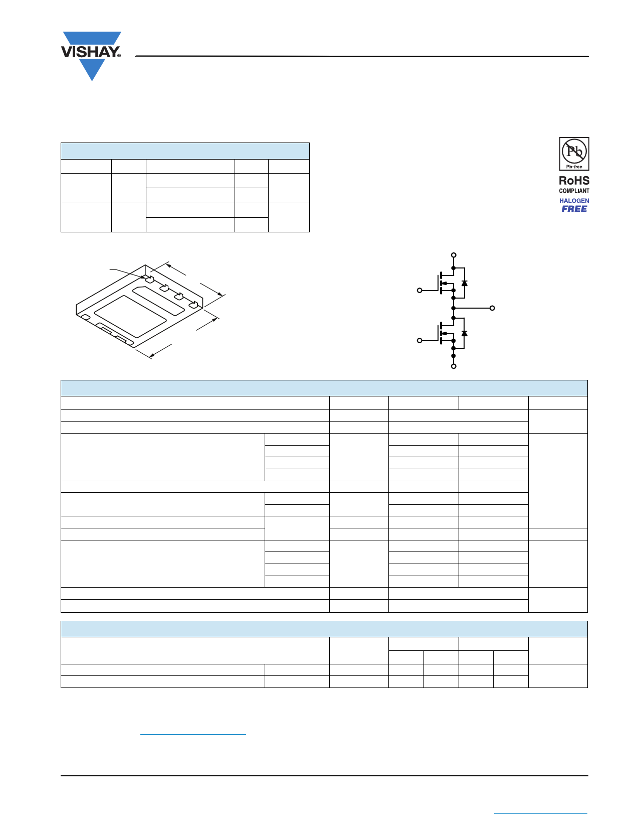
PowerPAIR® 6 x 5
Pin 1
1
G2
8
7
S1/D2
Pin 9
S2
6
5
G1
D1
5 mm
2 D1
D1 3
D1
4
6 mm
Ordering Information: SiZ902DT-T1-GE3 (Lead (Pb)-free and Halogen-free)
D1
G1
N-Channel 1
MOSFET
G2
N-Channel 2
MOSFET
S2
S1/D2
ABSOLUTE MAXIMUM RATINGS (TA = 25 °C, unless otherwise noted)
Parameter
Symbol
Channel-1
Channel-2
Drain-Source Voltage
Gate-Source Voltage
Continuous Drain Current (TJ = 150 °C)
Pulsed Drain Current (t = 300 µs)
Continuous Source Drain Diode Current
Single Pulse Avalanche Current
Single Pulse Avalanche Energy
Maximum Power Dissipation
Operating Junction and Storage Temperature Range
Soldering Recommendations (Peak Temperature)d, e
TC = 25 °C
TC = 70 °C
TA = 25 °C
TA = 70 °C
TC = 25 °C
TA = 25 °C
L = 0.1 mH
TC = 25 °C
TC = 70 °C
TA = 25 °C
TA = 70 °C
VDS
VGS
ID
IDM
IS
IAS
EAS
PD
TJ, Tstg
30
± 20
16a 16a
16a 16a
14.3b, c
11.4b, c
16a, b, c
16a, b, c
50
16a
3.4b, c
80
16a
4.1b, c
18 30
16 45
29 66
18 42
4.2b, c
2.7b, c
5b, c
3.2b, c
- 55 to 150
260
Unit
V
A
mJ
W
°C
THERMAL RESISTANCE RATINGS
Channel-1
Channel-2
Parameter
Symbol
Typ. Max. Typ. Max.
Unit
Maximum Junction-to-Ambientb, f
Maximum Junction-to-Case (Drain)
t 10 s
Steady State
RthJA
RthJC
24 30 20 25
3.4 4.3 1.5 1.9
°C/W
Notes:
a. Package limited.
b. Surface mounted on 1" x 1" FR4 board.
c. t = 10 s.
d. See solder profile (www.vishay.com/doc?73257). The PowerPAIR is a leadless package. The end of the lead terminal is exposed copper (not
plated) as a result of the singulation process in manufacturing. A solder fillet at the exposed copper tip cannot be guaranteed and is not required
to ensure adequate bottom side solder interconnection.
e. Rework conditions: manual soldering with a soldering iron is not recommended for leadless components.
f. Maximum under steady state conditions is 65 °C/W for channel-1 and 57 °C/W for channel-2.
Document Number: 63465
www.vishay.com
S11-2380 Rev. B, 28-Nov-11
1
This document is subject to change without notice.
THE PRODUCTS DESCRIBED HEREIN AND THIS DOCUMENT ARE SUBJECT TO SPECIFIC DISCLAIMERS, SET FORTH AT www.vishay.com/doc?91000
1 page 
New Product
SiZ902DT
Vishay Siliconix
CHANNEL-1 TYPICAL CHARACTERISTICS (25 °C, unless otherwise noted)
100 0.030
0.025
ID = 13.8 A
10
TJ = 150 °C
1
TJ = 25 °C
0.020
0.015
0.010
TJ = 125 °C
TJ = 25 °C
0.005
0.1
0.0 0.2 0.4 0.6 0.8 1.0
VSD - Source-to-Drain Voltage (V)
Source-Drain Diode Forward Voltage
1.2
1.9
1.8
1.7
1.6
ID = 250 µA
1.5
1.4
1.3
1.2
1.1
1.0
0.9
0.8
- 50 - 25
0 25 50 75 100 125 150
TJ - Temperature (°C)
Threshold Voltage
100 Limited by RDS(on*)
0.000
0
2468
VGS - Gate-to-Source Voltage (V)
On-Resistance vs. Gate-to-Source Voltage
10
50
40
30
20
10
0
0.001
0.01 0.1 1 10
Time (s)
Single Pulse Power
100 1000
10 100 μs
1 ms
1 10 ms
0.1
TA = 25 °C
BVDSS Limited
100 ms
1s
10 s
DC
0.01
0.1 1 10
VDS - Drain-to-Source Voltage (V)
* VGS > minimum VGS at which RDS(on) is specified
100
Safe Operating Area, Junction-to-Ambient
Document Number: 63465
www.vishay.com
S11-2380 Rev. B, 28-Nov-11
5
This document is subject to change without notice.
THE PRODUCTS DESCRIBED HEREIN AND THIS DOCUMENT ARE SUBJECT TO SPECIFIC DISCLAIMERS, SET FORTH AT www.vishay.com/doc?91000
5 Page 
New Product
CHANNEL-2 TYPICAL CHARACTERISTICS (25 °C, unless otherwise noted)
SiZ902DT
Vishay Siliconix
1
Duty Cycle = 0.5
0.2
0.1
0.1
0.05
0.02
0.01
0.0001
1
Single Pulse
Notes:
PDM
t1
t2
1. Duty Cycle, D =
t1
t2
2. Per Unit Base = RthJA = 57 °C/W
3. TJM - TA = PDMZthJA(t)
4. Surface Mounted
0.001
0.01
0.1
1
10
Square Wave Pulse Duration (s)
Normalized Thermal Transient Impedance, Junction-to-Ambient
100
1000
Duty Cycle = 0.5
0.2
0.1
0.05
0.02
Single Pulse
0.1
0.0001
0.001
0.01
Square Wave Pulse Duration (s)
Normalized Thermal Transient Impedance, Junction-to-Case
0.1
Vishay Siliconix maintains worldwide manufacturing capability. Products may be manufactured at one of several qualified locations. Reliability data for Silicon
Technology and Package Reliability represent a composite of all qualified locations. For related documents such as package/tape drawings, part marking, and
reliability data, see www.vishay.com/ppg?63465.
Document Number: 63465
www.vishay.com
S11-2380 Rev. B, 28-Nov-11
11
This document is subject to change without notice.
THE PRODUCTS DESCRIBED HEREIN AND THIS DOCUMENT ARE SUBJECT TO SPECIFIC DISCLAIMERS, SET FORTH AT www.vishay.com/doc?91000
11 Page | ||
| Páginas | Total 14 Páginas | |
| PDF Descargar | [ Datasheet SIZ902DT.PDF ] | |
Hoja de datos destacado
| Número de pieza | Descripción | Fabricantes |
| SIZ902DT | Dual N-Channel 30V (D-S) MOSFET | Vishay |
| Número de pieza | Descripción | Fabricantes |
| SLA6805M | High Voltage 3 phase Motor Driver IC. |
Sanken |
| SDC1742 | 12- and 14-Bit Hybrid Synchro / Resolver-to-Digital Converters. |
Analog Devices |
|
DataSheet.es es una pagina web que funciona como un repositorio de manuales o hoja de datos de muchos de los productos más populares, |
| DataSheet.es | 2020 | Privacy Policy | Contacto | Buscar |